Plasma processing apparatus

a plasma processing and plasma technology, applied in the direction of electrical apparatus, electric discharge tubes, basic electric elements, etc., can solve the problems of reducing the energy of ions bombarding the focus ring, affecting the plasma density distribution of semiconductor wafers, and affecting the performance of plasma processing, so as to achieve the effect of suppressing the consumption of the focus ring and improving the plasma density distribution on the semiconductor wafer w

Inactive Publication Date: 2013-01-10
TOKYO ELECTRON LTD
View PDF6 Cites 13 Cited by
  • Summary
  • Abstract
  • Description
  • Claims
  • Application Information

AI Technical Summary

Benefits of technology

The present invention provides a plasma processing apparatus that can effectively suppress the consumption of a focus ring without significantly affecting the plasma process. The apparatus uses two different frequencies of power to generate plasma and attract ions. By applying a second high frequency power with a relatively low frequency to the main lower electrode, the electric field in the ion sheath formed around the focus ring is reduced, resulting in decreased consumption of the focus ring. Additionally, by applying a first high frequency power with a relatively high frequency to the processing space, the plasma density distribution on the substrate is improved. Overall, the apparatus suppresses the consumption of the focus ring without substantially affecting the process.

Problems solved by technology

Therefore, in the case of a second high frequency, it is relatively difficult to pass through a propagation path of the peripheral dielectric member and the focus ring, and is relatively easy to pass through a propagation path of the main dielectric member and the substrate.
As a consequence, the electric field in the ion sheath formed on the focus ring becomes relatively weak, thus decreasing the energy of ions bombarding the focus ring and suppressing the consumption of the focus ring.

Method used


Image

  • Plasma processing apparatus
  • Plasma processing apparatus
  • Plasma processing apparatus

Examples


Embodiment Construction

[0037]Hereinafter, embodiments of the present invention will be described with reference to FIGS. 1 to 15 which form a part hereof.

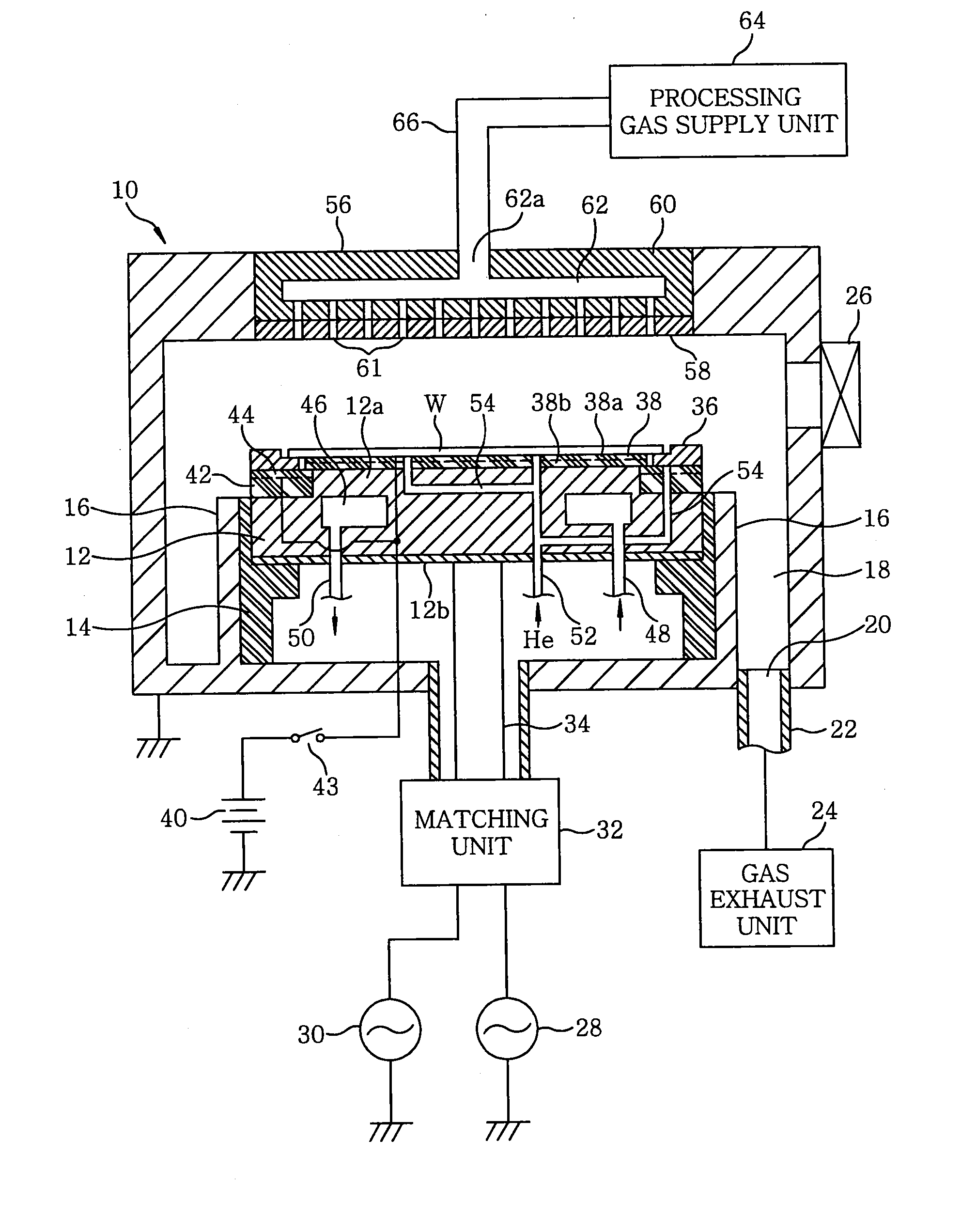
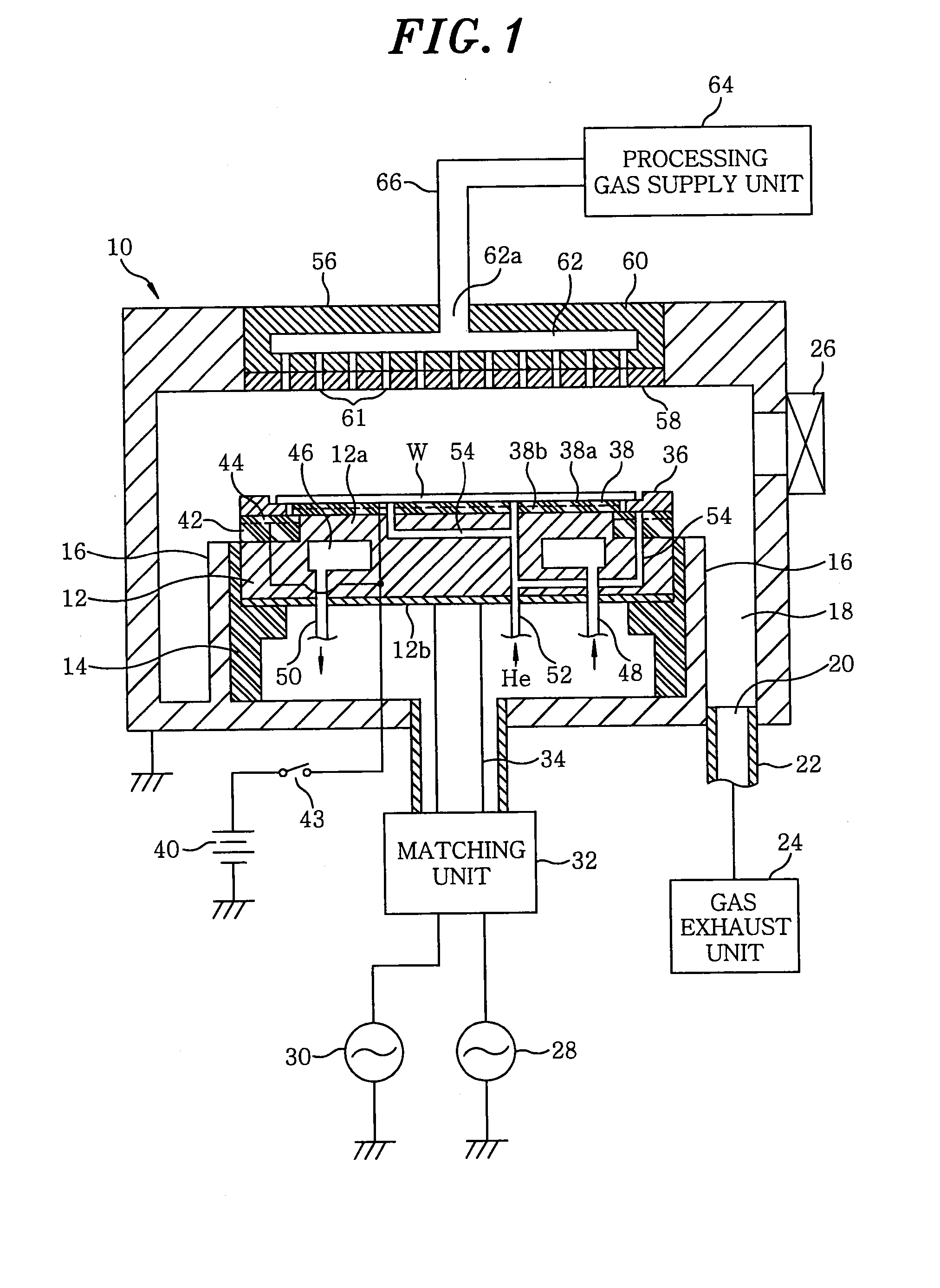
[0038]FIG. 1 is a vertical cross sectional view showing a configuration of a plasma etching apparatus in accordance with an embodiment of the present invention. This plasma etching apparatus is constructed as a capacitively coupled cathode couple plasma etching apparatus, and includes a cylindrical chamber (processing chamber) 10 made of a metal such as aluminum, stainless steel or the like. The chamber 10 is frame grounded.

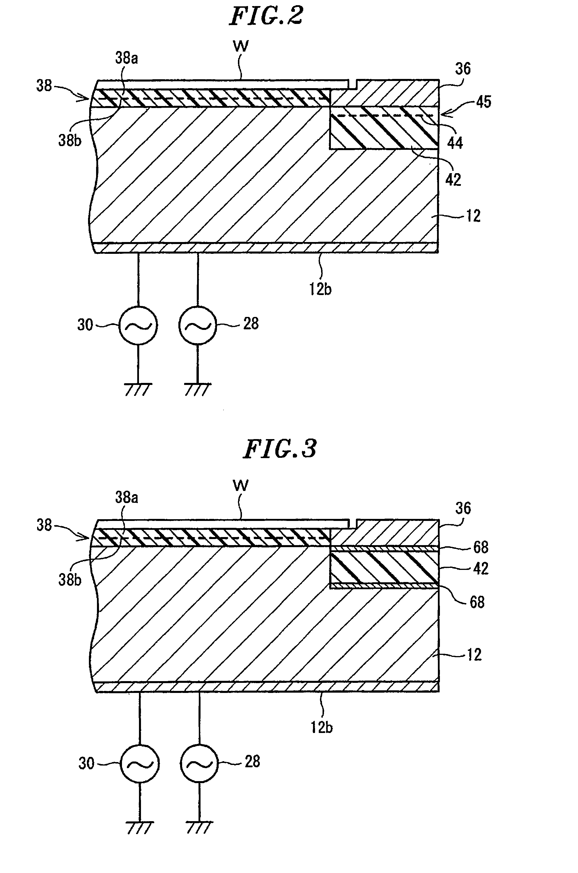
[0039]A circular plate-shaped susceptor 12 serving as a lower electrode for mounting thereon a target substrate, e.g., a semiconductor wafer W, is horizontally arranged in the chamber 10. The susceptor 12 has a main body or a base 12a made of, e.g., aluminum, and a conductive RF plate 12b fixed to a bottom surface of the base 12a. Further, the susceptor 12 is supported by a cylindrical insulating supporting portion 14 extending vertic...


PUM

PropertyMeasurementUnit
frequencyaaaaaaaaaa
frequencyaaaaaaaaaa
frequenciesaaaaaaaaaa

Abstract

A plasma processing apparatus includes a processing chamber, a first electrode and a second electrode disposed to face each other, a high frequency power supply unit for applying a high frequency power to either the first electrode or the second electrode, a processing gas supply unit for supplying a processing gas to a processing space, and a main dielectric member provided at a substrate mounting portion on a main surface of the first electrode. A focus ring is attached to the first electrode to cover a peripheral portion of the main surface of the first electrode and a peripheral dielectric member is provided in a peripheral portion on the main surface of the first electrode so that an electrostatic capacitance per unit area applied between the first electrode and the focus ring is smaller than that applied between the first electrode and the substrate by the main dielectric member.

Description

CROSS-REFERENCE TO RELATED APPLICATIONS[0001]This application is a divisional of U.S. application Ser. No. 12 / 056,665, filed Mar. 27, 2008, the entire content of which is incorporated herein by reference. U.S. application Ser. No. 12 / 056,665 is a non-provisional of U.S. Application Ser. No. 60 / 912,949, filed Apr. 20, 2007 and claims priority under 35 U.S.C. 119 to Japanese Application No. 2007-084706 filed Mar. 28, 2007.FIELD OF THE INVENTION[0002]The present invention relates to a technique for performing a plasma processing on a target substrate; and, more particularly, to a capacitively coupled plasma processing apparatus in which a focus ring is attached to an electrode for supporting a substrate.BACKGROUND OF THE INVENTION[0003]In a single sheet capacitively coupled plasma processing apparatus, a susceptor and a facing electrode (upper electrode) have diameters a little bit larger than that of a substrate in order to improve in-plane uniformity of a density of plasma (especiall...

Claims


Application Information

Patent Timeline
Patent Type & Authority Applications(United States)
IPC IPC(8): C23F1/08
CPCH01J37/32091H01J37/32642H01J37/32165H01J37/32155H01J37/32348H01J37/32449H01J37/32467H01J37/21H01J2237/21H01J2237/334
Inventor KOSHIMIZU, CHISHIOMATSUMOTO, NAOKITANAKA, SATOSHIITO, TORU
Owner TOKYO ELECTRON LTD
Why Eureka
Try Eureka