
Touch screen, manufacturing method thereof and display device

a technology of touch screen and display device, which is applied in the field of touch screen, can solve the problems of electrostatic capacitance failure and touch panel failure, and achieve the effects of improving electrostatic capacitance in the overlapping position, increasing the overlap area, and increasing the overlap capacitance therebetween

Active Publication Date: 2015-12-24
BOE TECH GRP CO LTD +1
View PDF5 Cites 2 Cited by
  • Summary
  • Abstract
  • Description
  • Claims
  • Application Information

AI Technical Summary

Benefits of technology

The present invention provides a touch screen with overlapping areas between connection lines to prevent failure caused by small electrostatic capacitance. The method involves overlapping the first and second sensing units with the corresponding connection lines to increase the overlapping area and improve the ability of anti-static electricity. Additionally, first and second branch lines are led out from the connection lines to further enhance the overlapping capacitance. This solution improves the manufacturing process and overall performance of the touch screen.

Problems solved by technology

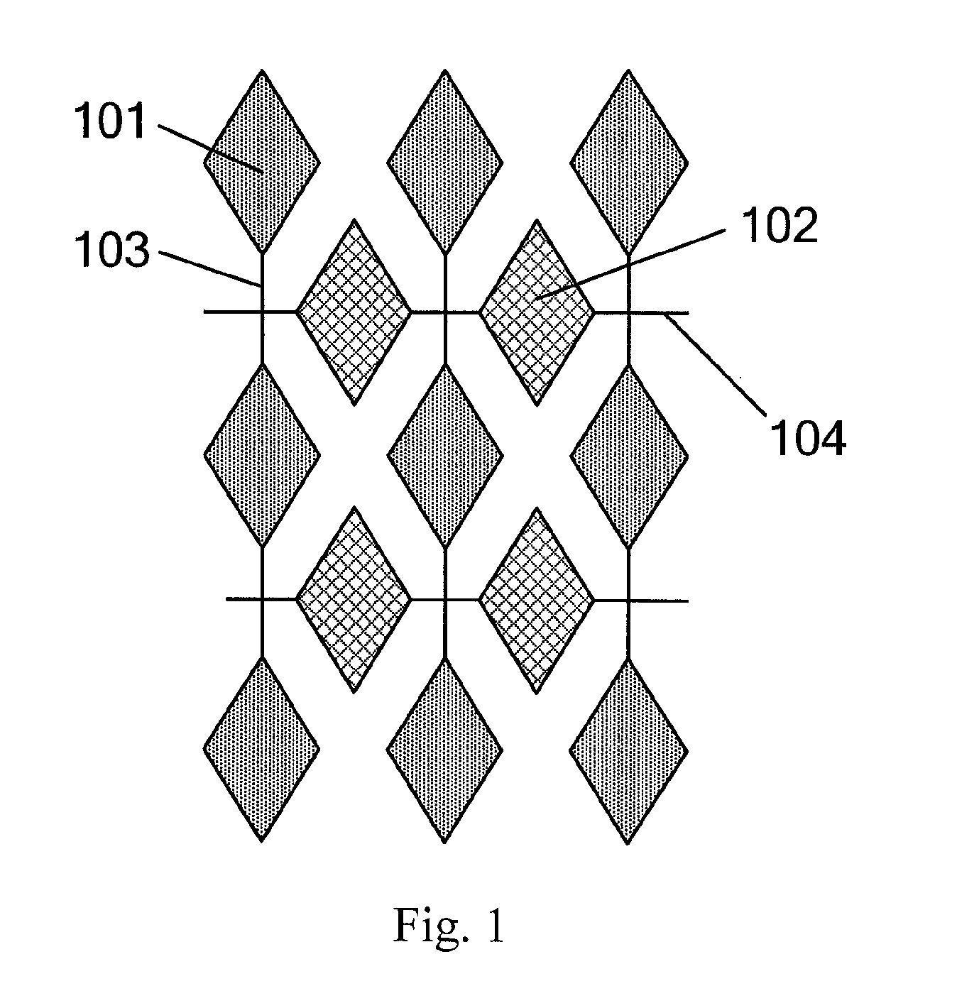
Further, since the overlapping area of the first connection line and the second connection line is relatively small and the resistance thereof is larger than that of the patter of the sensing unit, while the thickness of an insulated layer in the overlapping portion provided between the first connection line and the second connection line is relatively thin due to the limitation of the forming process of the thin film, the overlapping area between the first connection line and the second connection line readily renders electrostatic capacitance every small, and is apt to be damaged due to the static electricity and causes failure of the touch panel.

Method used


Image

  • Touch screen, manufacturing method thereof and display device
  • Touch screen, manufacturing method thereof and display device
  • Touch screen, manufacturing method thereof and display device

Examples


Embodiment Construction

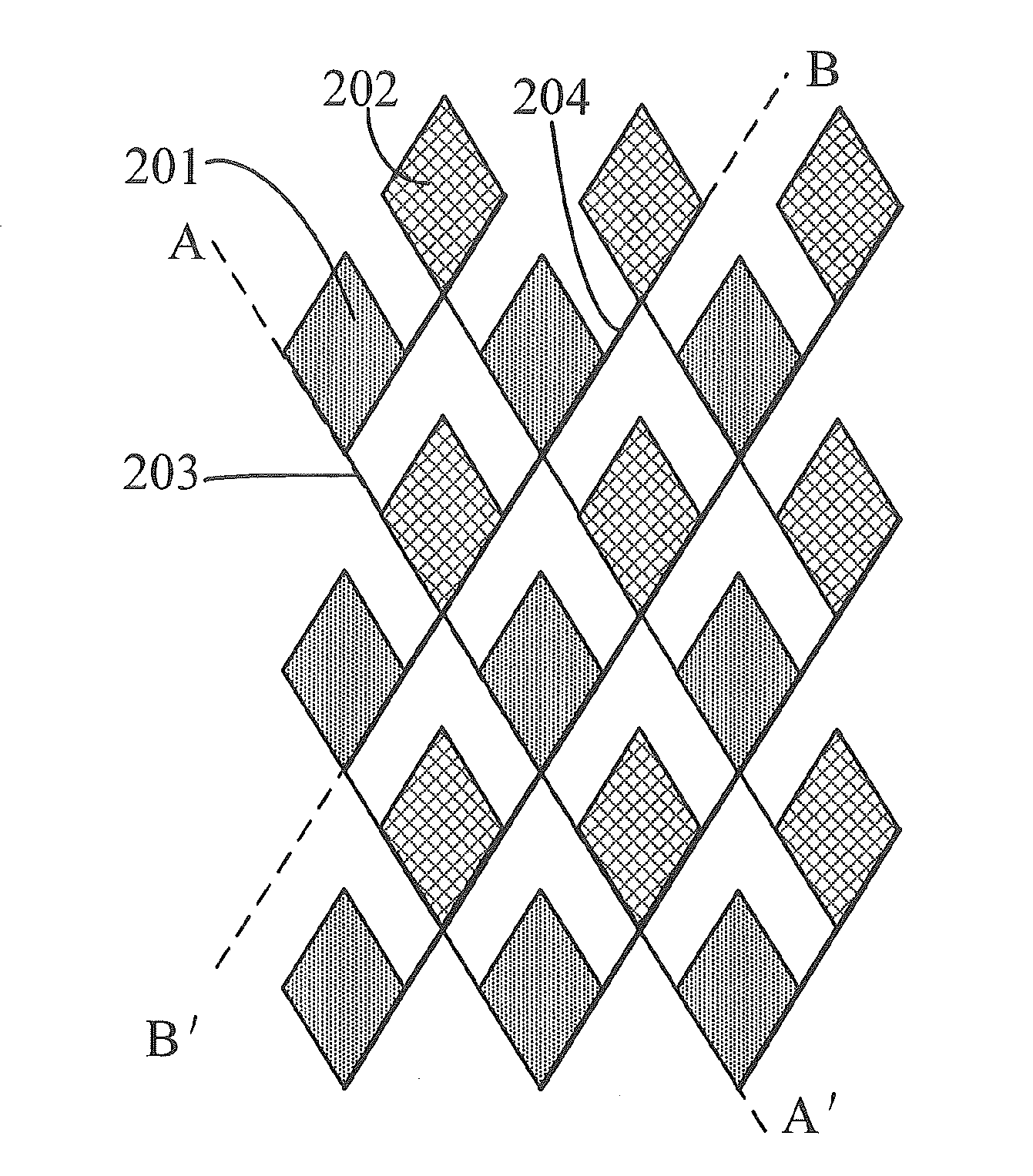
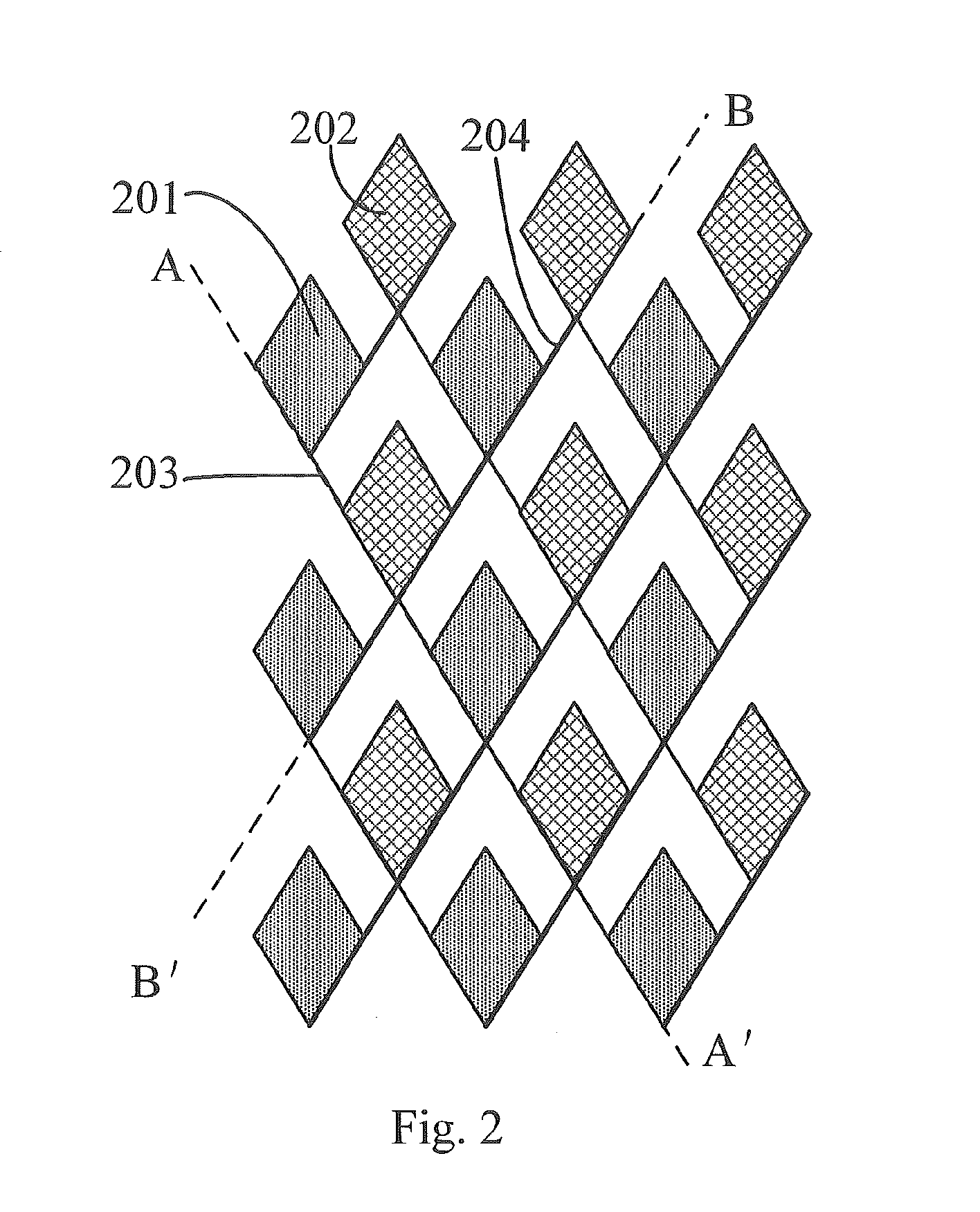
[0036]In order to completely understand the object, technical solution and advantages of the present invention, exemplary embodiments of the present disclosure will be described hereinafter in detail with reference to the attached drawings. FIG. 2 is the principal schematic view of arrangement of sensing units in a touch screen according to the first embodiment of the present invention. As shown in FIG. 2, the touch screen includes: a plurality of first sensing units 201 connected to each other by a first connection line 203 in a first direction AA′; and a plurality of second sensing units 202 connected to each other by a second connection line 204 in a second direction BB′. The first sensing units 201 and the second sensing units 202 are arranged alternatively in the first and second directions, and in the first direction, at least part of one second sensing units 202 is overlapped with the first connection line 203 between two first sensing units 201 adjacent to said one second se...


PUM


Abstract

A touch screen, a manufacturing method thereof and a display device are disclosed. In the touch screen, a plurality of first sensing units are connected to each other by a first connection line in a first direction; and a plurality of second sensing units are connected to each other by a second connection line in a second direction; the first sensing units and the second sensing units are arranged alternatively in the first and second direction; and in the first direction, at least part of the second sensing units is overlapped with the first connection line between two first sensing units adjacent to this second sensing unit, and in the second direction, at least part of the first sensing units is overlapped with the second connection line between two second sensing units adjacent to this first sensing unit. The overlapping area between the first sensing unit and the respective connection line and the overlapping area between the second sensing unit and the respective connection line is increased, improving the electrostatic capacitance in the overlapping position, and in turn improving the ability of anti-static electricity of the touch screen.

Description

BACKGROUND OF THE INVENTION[0001]1. Field of the Invention[0002]Embodiments of the present invention relate to a touch screen of a display device, more particularly, relates to a touch screen, a manufacturing method thereof and a display device including the same.[0003]2. Description of the Related Art[0004]A touch panel is an input device, which allows to input user's instructions therein by selecting the instruction contents displayed on a screen, such as an image display device, by means of a finger of the user or an object. Generally, the touch panel is provided in front of the image display device so as to transfer a contact position into an electrical signal. In this way, the finger of the user or the object directly comes into contact with the touch panel at the contact position. Therefore, the instruction content selected at the contact position is inputted into the image display device as an input signal. Since such touch panel has been used to replace a separate input devi...

Claims


Application Information

Patent Timeline
Patent Type & Authority Applications(United States)
IPC IPC(8): G06F3/044G06F1/16G06F3/041
CPCG06F3/044G06F3/0412G06F2203/04103G06F2203/04111G06F1/16G06F3/0446G06F3/0445
Inventor WANG, BENLIAN
Owner BOE TECH GRP CO LTD
Learn More