Vibrating element, vibrator, oscillator, and electronic device

Active Publication Date: 2012-09-13
SEIKO EPSON CORP
View PDF9 Cites 22 Cited by
  • Summary
  • Abstract
  • Description
  • Claims
  • Application Information

AI Technical Summary

Benefits of technology

[0026]By providing the projection sections on the both principal surfaces in the area on the piezoelectric substrate where the vibratory displacement is sufficiently attenuated, there is an advantage that the possibility for the excitation electrodes provided to the excitation section to have contact with the inner surface of the package when installing the element to the package can be eliminated. Further, according to the vibrating element using the piezoelectric substrate, there is an advantage that the combination of the thickness-shear vibration and the unwanted mode such as a contour vibration in a direction perpendicular to the plane having the non-stepped shape can be suppressed to thereby reduce the CI value.Application Example 2
[0056]According to the configuration of the electronic device described above, since the electronic device is configured using at least one electronic component among the thermistor, the capacitor, the reactive element, and the semiconductor element, and the piezoelectric vibrating element, there is an advantage that the electronic device becomes a useful device for electronic equipment.

Problems solved by technology

However, in the piezoelectric vibrator having smaller length-to-thickness ratio, there is a problem that the vibratory displacement is not sufficiently attenuated in an end portion of the X axis to thereby excite the unwanted flexural mode in the end surface, which is combined with the principal vibration.
However, since the package shape is small, there is a problem that a necessary amount of electrically-conductive adhesive fails to be provided to thereby easily degrade the adhesion force, and thus the principal surface of the piezoelectric vibrating element is tilted, and the excitation electrodes have contact with an inner bottom of the package to thereby cause a malfunction.
In the quartz crystal vibrating element of Document 13, there is a problem that although the thick-wall projection section provided to the one edge thereof in the longitudinal direction (the X-axis direction) has the function of preventing the excitation electrodes and the package from having contact with each other, some of the vibratory displacement energy of the quartz crystal vibrating element is lost due to the interference with the thick-wall projection section provided to the one edge.
The smaller the quartz crystal vibrating element is made, the larger the influence rate of the loss becomes, and there is a problem that it is difficult to stabilize the electrical characteristics of the quartz crystal vibrator.
However, in the thickness-shear vibrating element using a quartz crystal substrate having a multistage mesa structure with the long-side direction parallel to the X axis (the electrical axis as one of the crystal axes of the quartz crystal), there is a problem that in the condition in which the X length-to-thickness ratio (the ratio X / t of the long-side dimension X to the thickness t) is low, for example, the ratio X / t is equal to or lower than 17, there occurs the combination of the thickness-shear vibration and contour vibration (e.g., a flexural vibration) in a direction parallel to a Z′ axis (an axis obtained by rotating an optical axis as one of the crystal axes of the quartz crystal as much as a predetermined angle taking the X axis as the central axis).
On this occasion, there is a problem that it is difficult to keep the both principal surfaces of the quartz crystal vibrating element and the bottom of the package parallel to each other due to the amount and the viscosity of the electrically-conductive adhesive applied to the element mounting pad, and the excitation electrodes of the quartz crystal vibrating element have contact with the bottom of the package or the lid member for seal to thereby deteriorate the electrical characteristics of the quartz crystal vibrator.

Method used


Image

  • Vibrating element, vibrator, oscillator, and electronic device
  • Vibrating element, vibrator, oscillator, and electronic device
  • Vibrating element, vibrator, oscillator, and electronic device

Examples


first embodiment

of the Invention

[0100]A first embodiment of the invention will hereinafter be explained with reference to the accompanying drawings. The invention is not at all limited by the embodiment described below, and includes a variety of types of modified examples put into practice within a scope or spirit of the invention. It should be noted that all of the constituents described in the following embodiment below are not necessarily essential elements of the invention.

1. Piezoelectric Vibrating Element (Vibrating Element)

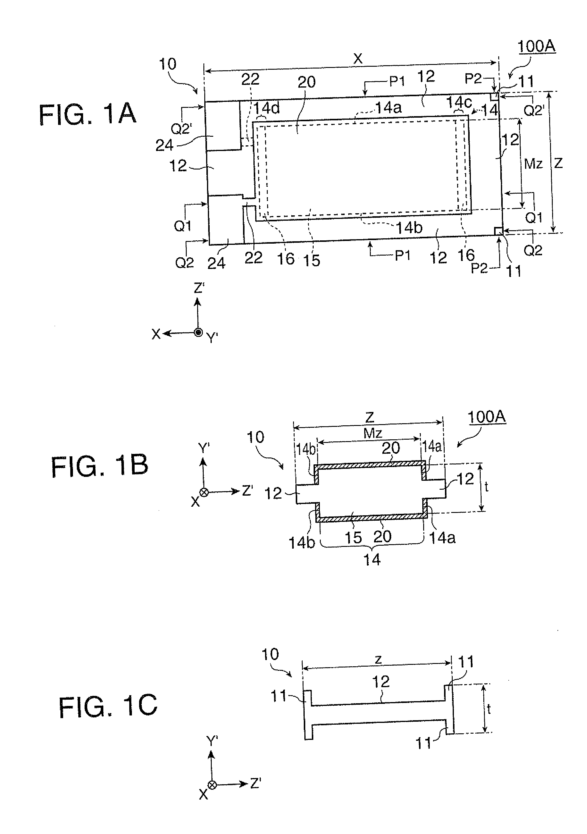
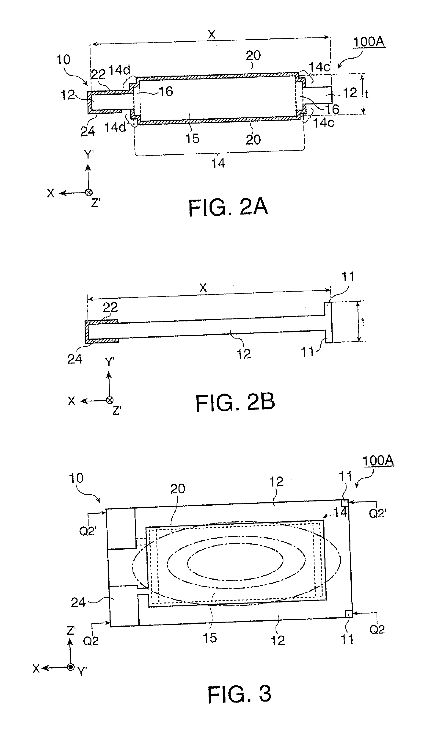
[0101]Firstly, a piezoelectric vibrating element according to the present embodiment will be explained with reference to the accompanying drawings. FIGS. 1A through 1C, 2A, and 2B are schematic diagrams showing a configuration of a piezoelectric vibrating element (a vibrating element) 100A according to an embodiment of the invention. FIG. 1A is a plan view of the piezoelectric vibrating element 100A, FIG. 1B is a P1-P1 cross-sectional view of FIG. 1A, and FIG. 1C is a P2-P...

second embodiment

of the Invention

[0188]Then, a second embodiment of the invention will hereinafter be explained with reference to the accompanying drawings.

1. Piezoelectric Vibrating Element (Vibrating Element)

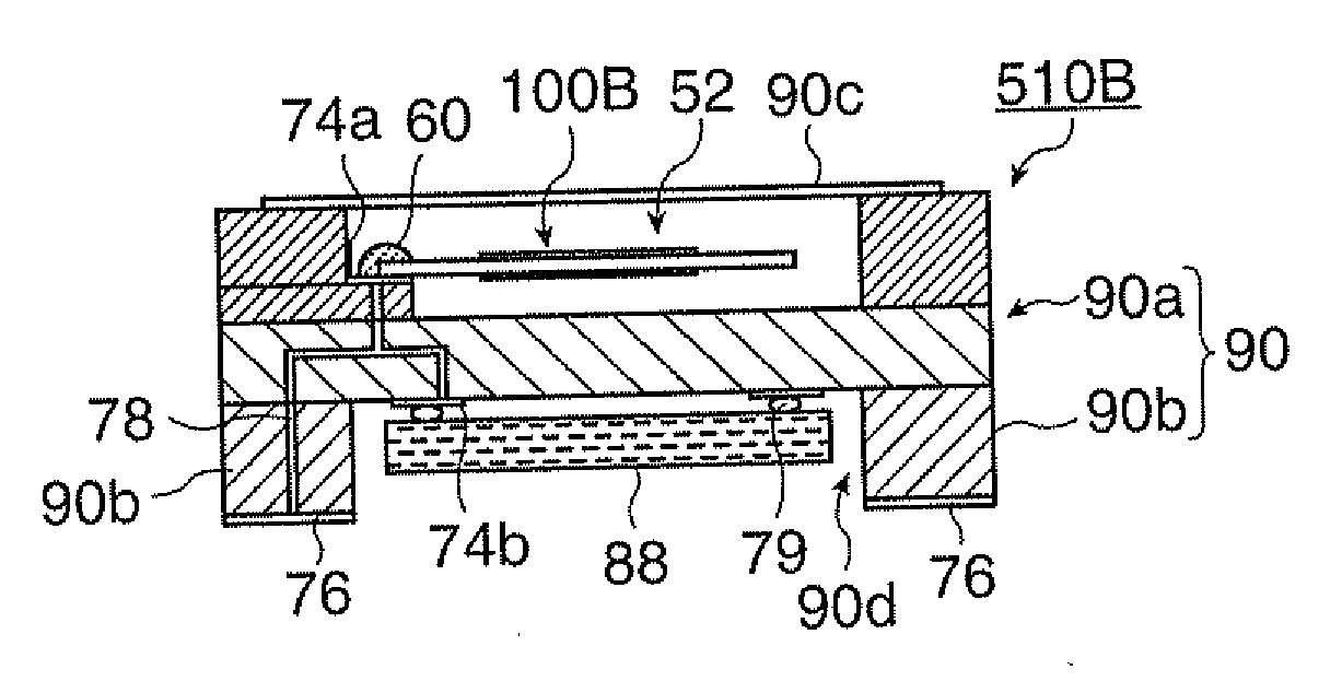
[0189]Firstly, a piezoelectric vibrating element according to the present embodiment will be explained with reference to the accompanying drawings. FIGS. 23A through 23C, 24A, and 24B are schematic diagrams showing a configuration of a piezoelectric vibrating element 100B according to the second embodiment of the invention. FIG. 23A is a plan view of the piezoelectric vibrating element 100B, FIG. 23B is a P1-P1 cross-sectional view of FIG. 23A, and FIG. 230 is a P2-P2 cross-sectional view of FIG. 23A. FIG. 24A is a Q1-Q1 cross-sectional view of FIG. 23A, and FIG. 24B is a Q2-Q2 cross-sectional view or a Q2′-Q2′ cross-sectional view of FIG. 23A.

[0190]The piezoelectric vibrating element 100B according to the second embodiment is provided mainly with a piezoelectric substrate 10 having a excitati...

experimental example

5. Experimental Example

[0251]Hereinafter, an experimental example will be shown, and the present embodiment will more specifically be explained. It should be noted that the scope of the invention is not at all limited by the following experimental example.

5.1 Configuration of Piezoelectric Vibrating Element

[0252]As a specific example, the piezoelectric vibrating element 100B having the two-stage mesa structure shown in FIGS. 23A through 23C, 24A, and 24B is used. Specifically, the AT-cut quartz crystal substrate is processed by a wet-etching process using a solution including hydrofluoric acid to thereby form the piezoelectric substrate 10 having the peripheral section 12 and the excitation section 14. The piezoelectric substrate 10 is formed to be symmetrical about a point (not shown) to be the center of symmetry. The thickness t of the first part 15 of the excitation section 14 is set to 0.065 mm, and the vibrational frequency is set to 24 MHz. Further, the dimension X of the long...


PUM


Abstract

A vibrating element includes a piezoelectric substrate having an excitation section adapted to excite a thickness-shear vibration, and provided with a step section in each of side surfaces on both ends, and a peripheral section having a thickness smaller than a thickness of the excitation section, and the peripheral section has at least one projection section disposed on both principal surfaces in an area where a vibratory displacement when the excitation section excites a vibration is sufficiently attenuated.

Description

BACKGROUND[0001]1. Technical Field[0002]The present invention relates to a thickness vibration mode piezoelectric vibrator, and in particular to a piezoelectric vibrating element (a vibrating element), a piezoelectric vibrator (a vibrator), a piezoelectric oscillator (an oscillator), and an electronic device each having a so-called mesa structure.[0003]2. Related Art[0004]A quartz crystal vibrating element using an AT-cut quartz crystal vibrating element has the vibration mode of thickness-shear vibration, and has frequency temperature characteristics showing an excellent cubic curve, and is therefore used in a number of fronts such as electronic equipment.[0005]JP-A-58-047316 (Document 1) discloses a piezoelectric vibrator (an AT-cut quartz crystal vibrator) of a so-called mesa structure having the same level of energy confinement effect as that of the bevel structure or the convex structure.[0006]It is known that, in the thickness-shear vibrator having a small length-to-thickness ...

Claims


Application Information

Patent Timeline
IPC IPC(8): H03B5/32H01L41/04
CPCH03H3/02H03H9/02023H03H9/02086H03H9/02149H03H9/02157H03H2003/022H03H9/0542H03H9/0547H03H9/0552H03H9/1021H03H9/19H03H9/0509H03H9/177H03B5/36
Inventor II, TOSHIHIRONAITO, MATSUTARO
Owner SEIKO EPSON CORP
Why Eureka
Try Eureka