
Uniform multilayer graphene by chemical vapor deposition

Active Publication Date: 2012-09-06
RGT UNIV OF MICHIGAN
View PDF3 Cites 21 Cited by
  • Summary
  • Abstract
  • Description
  • Claims
  • Application Information

AI Technical Summary

Benefits of technology

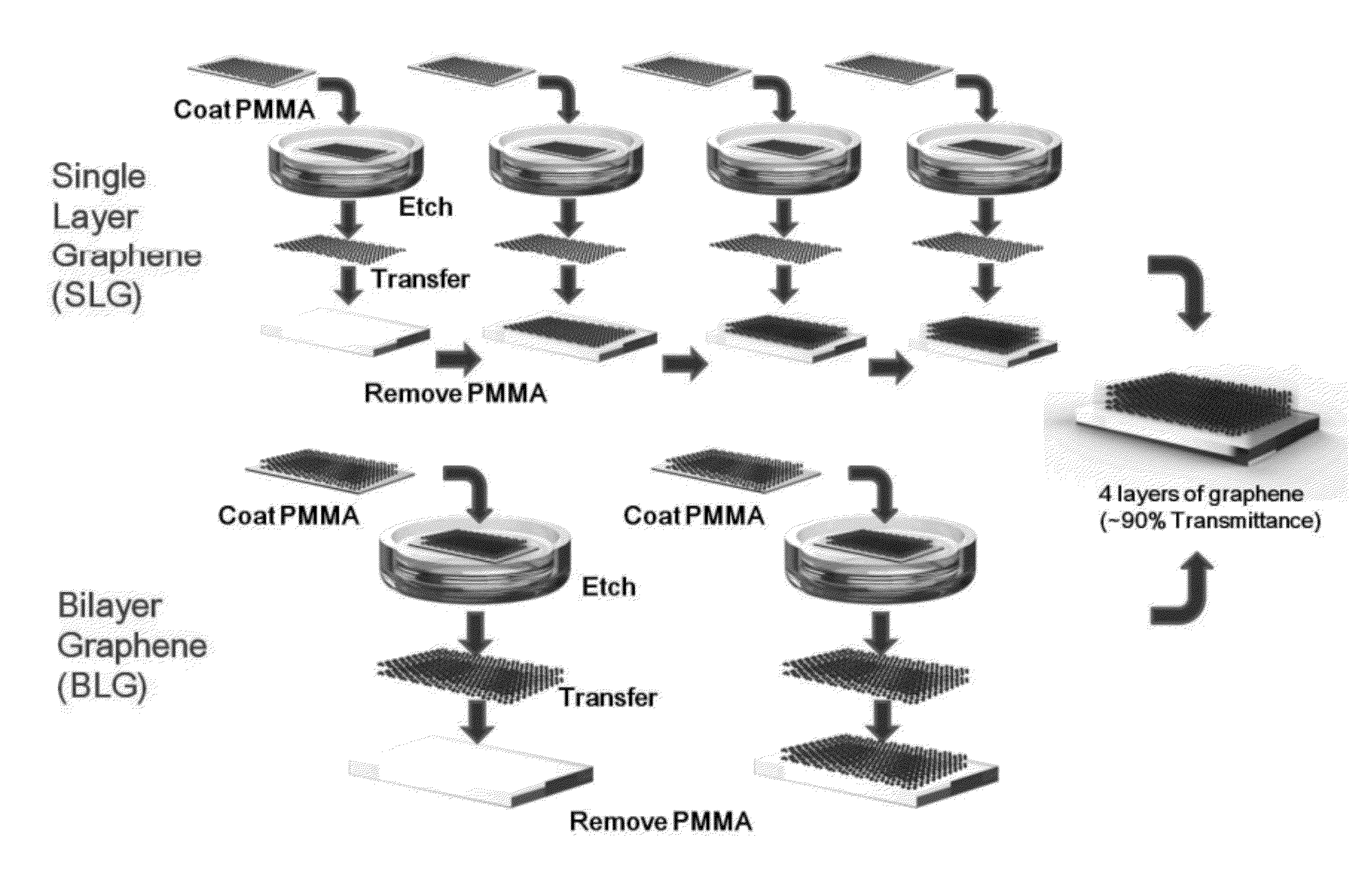
[0008]In accordance with another embodiment, a method of producing multilayer graphene is provided. The method comprises the steps of: (a) placing a substrate having a metal surface in a reaction chamber of a furnace; (b) flowing H2 gas in the reaction chamber; (c) increasing the temperature in the reaction chamber to a desired level; (d) after the temperature in the reaction chamber reaches the desired level, ceasing flow of the H2 gas, and flowing reaction gas in the reaction chamber for a desired time; and (e) after the desired time, decreasing the temperature in the reaction chamber at a controlled rate.
[0009]In accordance with another embodiment, a method of producing multilayer graphene is

Problems solved by technology

This can lead to high processing time and cost, and a higher likelihood of defects in the films.
BLG has also been fabricated via mechanical exfoliation of graphite to produce SLG that is subsequently stacked with another SLG, but the sheet size is limited to the square-micron range and such processes are not scalable to sizes large enough to be practical for use in many electronics applications.
The synthesis of wafer scale uniform bilayer graphene product presents a tremendous challenge.
Multiple layer graphene (MLG) structures produced by these methods typically have non-uniform thickness, with different numbers of graphene layers throughout the structure, and rough surfaces compared to LPCVD-grown SLG.
Graphene sheet thickness variation can be problematic for use in electronics applications because it causes the sheet resistance and optical transmittance to vary among different areas of the sheet.
Additionally, APCVD processes that are used to produce MLG can lead to higher numbers of defects compared to LPCVD SLG due to particulate deposition resulting from APCVD conditions.

Method used


Image

  • Uniform multilayer graphene by chemical vapor deposition
  • Uniform multilayer graphene by chemical vapor deposition
  • Uniform multilayer graphene by chemical vapor deposition

Examples


Embodiment Construction

[0045]Described below are exemplary embodiments of a method of producing uniform multilayer graphene by chemical vapor deposition (CVD), as well as exemplary graphene structures and products that may be constructed using the method. Uniform multilayer graphene may be directly synthesized or grown on a CVD substrate in a CVD reaction chamber. As such, the multiple graphene layers may be deposited in a single CVD process or process cycle without the need to produce multiple separate monolayers and then stack the monolayers on top of one another. Uniform bilayer graphene (BLG) can be produced using one embodiment of the method. Multilayer graphene produced as described herein may be further characterized by interlayer uniformity due to the nature of CVD processes and the manner in which the individual carbon atoms self-organize in such a process. Certain embodiments of the method may be expanded to include fabrication of flexible transparent conductors from CVD-produced multilayer grap...


PUM

PropertyMeasurementUnit
Temperatureaaaaaaaaaa
Pressureaaaaaaaaaa

Abstract

A method of producing uniform multilayer graphene by chemical vapor deposition (CVD) is provided. The method is limited in size only by CVD reaction chamber size and is scalable to produce multilayer graphene films on a wafer scale that have the same number of layers of graphene throughout substantially the entire film. Uniform bilayer graphene may be produced using a method that does not require assembly of independently produced single layer graphene. The method includes a CVD process wherein a reaction gas is flowed in the chamber at a relatively low pressure compared to conventional processes and the temperature in the reaction chamber is thereafter decreased relatively slowly compared to conventional processes. One application for uniform multilayer graphene is transparent conductors. In processes that require multiple transfers of single layer graphene to achieve multilayer graphene structures, the disclosed method can reduce the number of process steps by at least half.

Description

CROSS-REFERENCE TO RELATED APPLICATION[0001]This application claims the benefit of U.S. Provisional Patent Application No. 61 / 379,925, filed Sep. 3, 2010, the complete disclosure of which is hereby incorporated by reference.TECHNICAL FIELD[0002]This invention relates generally to elemental carbon compositions and, more particularly, to graphene, methods of producing graphene, and products having graphene.BACKGROUND OF THE INVENTION[0003]Single and few-layer graphene has emerged as a promising material for novel applications in electronics due to certain advantageous optical and electrical properties and due to its potential for integrating bottom-up nanomaterial synthesis with top-down lithographic fabrication at a wafer size or macro scale. Its semi-metallic nature with high carrier mobility and low opacity also makes it a good candidate for use as transparent conductors for photovoltaic devices, touch panels, and displays, for example. Graphene structures also have high chemical r...

Claims


Application Information

Patent Timeline
IPC IPC(8): B32B9/04H01L29/12B32B37/14C23C16/26H01B1/04H01L21/20C23C16/01B82Y40/00B82Y99/00
CPCB82Y30/00Y10T428/30C01B31/0446C01B31/0453C01B2204/32C23C16/0209C23C16/26C23C16/45502C23C16/45557H01L21/02381H01L21/02425H01L21/02488H01L21/02527H01L21/0262B82Y40/00C01B32/184C01B32/186
Inventor ZHONG, ZHAOHUILEE, SEUNGHYUNLEE, KYUNGHOON
Owner RGT UNIV OF MICHIGAN
Learn More