Trench mosfet with super pinch-off regions and self-aligned trenched contact

a technology of trench mosfet and self-aligning, which is applied in the direction of semiconductor devices, diodes, electrical devices, etc., can solve the problems of reducing cell pitch and constraining cell pitch shrinkage, so as to reduce qgd, reduce on-resistance, and improve the effect of doping concentration

Inactive Publication Date: 2012-07-12
FORCE MOS TECH CO LTD
View PDF17 Cites 19 Cited by
  • Summary
  • Abstract
  • Description
  • Claims
  • Application Information

AI Technical Summary

Benefits of technology

[0007]It is therefore an object of the present invention to provide a new and improved semiconductor power device such as a trench MOSFET with two type gate trenches for device shrinkage by forming self-aligned contact and super pinch-off regions for reduced on-resistance by forming short channel. Briefly, in a preferred embodiment, this invention discloses a power semiconductor device comprising: a plurality of first type gate trenches extending into a silicon layer of a first conductivity type; a plurality of second type gate trenches extending into the silicon layer and formed symmetrically and disposed below the first type gate trenches, each second type gate trench having narrower trench width than the first type gate trench, and each second type gate trench surrounded by source regions of the first conductivity type and body regions of a second conductivity type adjacent opposing sidewalls of each second type gate trench in upper portion of the silicon layer; a gate electrode filled in the second type gate trenches; a dielectric layer filled in the first type gate trenches symmetrically over the gate electrode; a gate insulating layer insulating the gate electrode from adjacent body regions, source regions and silicon layer; a plurality of source-body contact trenches formed between two adjacent of the first type gate trenches and penetrating through the source regions and the body regions and extending into the silicon layer between two adjacent of the second type gate trenches; and an anti-punch through region of said second conductivity type surrounding sidewall and bottom of each source-body contact trench below the source region.
[0008]In order to further reduce Qgd, a shield electrode is disposed in lower portion of gate trenches in some embodiments connecting to a source metal. Briefly, in another preferred embodiment, this invention discloses a power semiconductor device comprising: a plurality of first type gate trenches extending into a silicon layer of a first conductivity type; a plurality of second type gate trenches extending into the silicon layer and formed symmetrically disposed below the first type gate trenches, each second type gate trench having narrower trench width than the first type gate trench, and each second type gate trench surrounded by source regions of the first conductivity type and body regions of a second conductivity type adjacent opposing sidewalls of each second type gate trench in upper portion of the silicon layer; a gate electrode and a shield electrode disposed in the second type gate trench, wherein the gate electrode and the shield electrode insulated from each other by an inter-electrode insulation layer and from adjacent body regions, source regions and silicon layer by gate insulating layers, wherein the source regions and the body regions being adjacent to the gate electrode; the gate electrode connected to a gate metal and shield electrode to a source metal; a dielectric layer filled in the first type gate trenches symmetrically over the gate electrode; a plurality of source-body contact trenches formed between two adjacent of the first type gate trenches and penetrating through the source regions and the body regions and extending into the silicon layer between two adjacent of the second type gate trenches; and an anti-through punch-through region of the second conductivity type surrounding sidewall and bottom of each source-body contact trench below the source region.
[0009]In other preferred embodiments, this invention can be implemented including one or more of following features: each second type gate trench symmetrically disposed below each first type gate trench; the gate electrode is doped poly-silicon layer; the power semiconductor device further comprises a tungsten layer padded by a barrier layer filled into each source-body contact trench for contacting the source regions and the body regions along sidewalls of the source-body contact trenches, the tungsten layer electrically connected to a source metal; the tungsten layer in FIG. 8 is only filled within each source-body contact trench but not extended over on top surface of the dielectric layer filled in first type gate trenches; the tungsten layer in some embodiment is not only filled within each source-body contact trench but also further extended over top surface of the dielectric layer filled in first type gate trenches; the power semiconductor device further comprises a source metal over the silicon layer and the tungsten layer, wherein the source metal electrically connected to the tungsten layer; the power semiconductor device further comprises an on-resistance reduction implanted region of the first conductivity type extending between two adjacent of the second type gate trenches below the body regions for further Rds reduction, the on-resistance reduction region having higher doping concentration than the silicon layer; the power semiconductor device further comprises at least one implanted pinch-off island of the second conductivity type in the silicon layer underneath the anti-punch through region and between two adjacent of the gate electrodes for further Idsx reduction; the source metal is Al alloys or Cu layer; the source metal is Ni / Ag or Ni / Au layer; the source metal is composed of a Ni / Au or Ni / Ag over a Al alloys layer; the power semiconductor device further comprises a resistance reduction layer such as Ti or Ti / TiN layer underneath the source metal; the source-body contact trenches are self-aligned to the first type gate trenches; the silicon layer is an epitaxial layer of the first conductivity type supported onto a substrate of the first conductivity type, wherein the epitaxial layer having lower doping concentration than the substrate; the gate electrode and shield electrode are doped poly-silicon layers, and the shield electrode has lower doping concentration than the gate electrode; the power semiconductor device further comprises a parasitic resistor disposed between the shield electrode and the source metal, the parasitic resistor has a resistance from 0.5 ohms to 200 ohms adjusted by sheet resistance of the shield electrode; the power semiconductor device further comprises at least one implanted pinch-off island of the second conductivity type in the silicon layer underneath the anti-punch through region and between two adjacent of the shield electrodes for further Idsx reduction; the gate insulating layers comprises a thicker oxide layer on bottom and sidewalls of the shield electrodes and a thinner oxide layer on sidewalls of the gate electrodes.
[0010]This invention further disclosed a method of manufacturing a power semiconductor device with two type gate trenches for device shrinkage by forming self-aligned contact and super pinch-off regions for reduced on-resistance by forming a short channel comprising the steps of: forming a plurality of first type gate trenches extending into a silicon layer; then forming a plurality of second type gate trenches in the silicon layer and symmetrically disposed below the first type gate trenches, wherein the second type gate trenches having narrower trench width than the first type gate trenches; forming body regions having opposite conductivity type to the silicon layer between two adjacent of the first type gate trenches and in upper portion of the silicon layer between two adjacent of the second type gate trenches; forming a dielectric layer within the first type gate trenches; removing portion of the body regions from spaces between two adjacent of the first type gate trenches; then forming source regions having opposite conductivity type to the body regions in upper portion of the body regions; forming a plurality of source-body contact trenches along sidewalls of the first type gate trenches and penetrating through the source regions and the body regions and extending into the silicon layer between two adjacent of the second type gate trenches, wherein the source-body contact trenches are self-aligned to the first type gate trenches; forming an anti-punch through region surrounding bottom and sidewall of each source-body contact trench below the source region.

Problems solved by technology

For power MOSFETs, which are well known in the semiconductor industry, reducing the cell pitch is one of the most challenging technologies to those skilled in the art.
However, there are still some disadvantages constraining the shrinkage of the cell pitch.

Method used


Image

  • Trench mosfet with super pinch-off regions and self-aligned trenched contact
  • Trench mosfet with super pinch-off regions and self-aligned trenched contact
  • Trench mosfet with super pinch-off regions and self-aligned trenched contact

Examples


Embodiment Construction

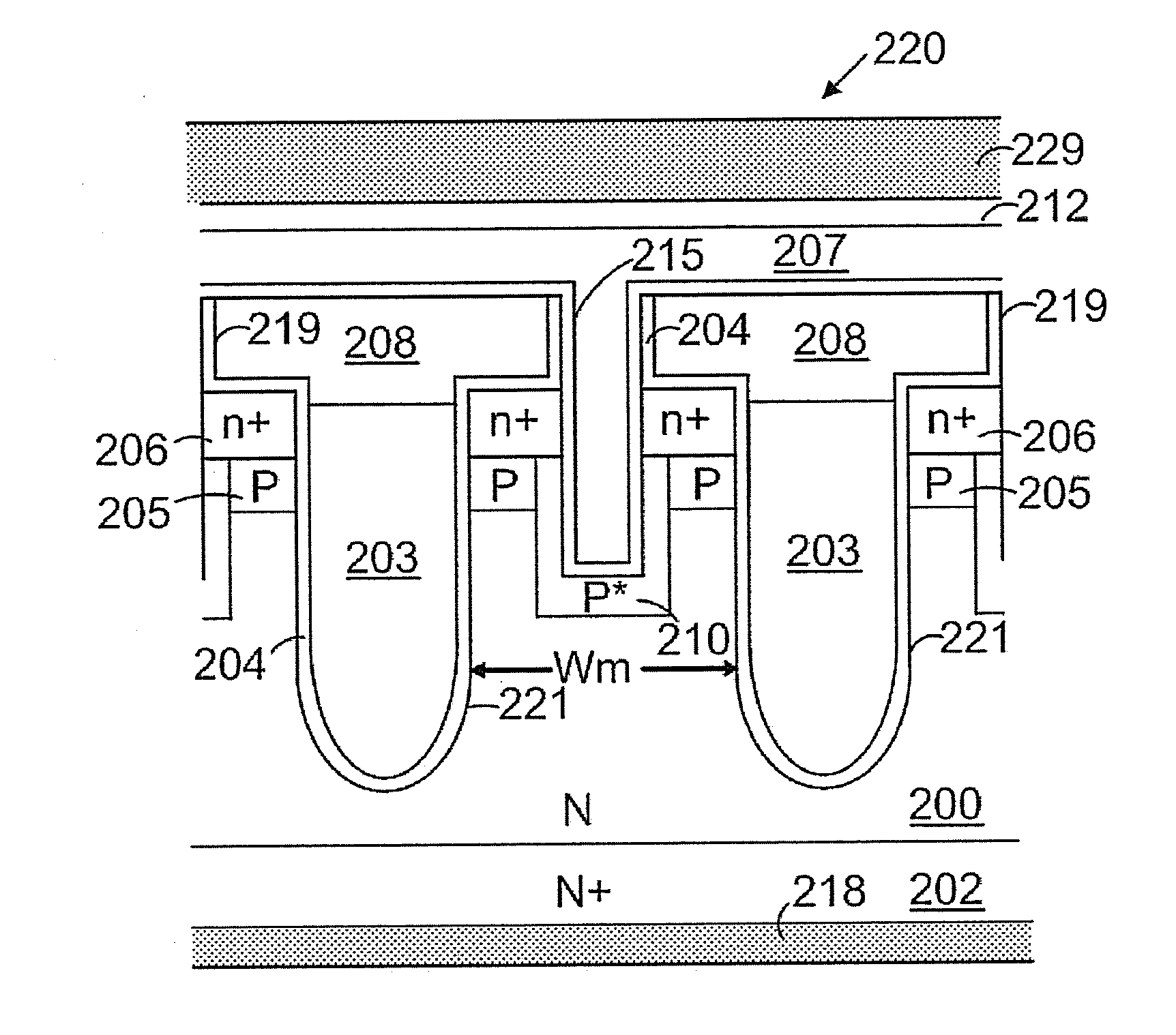
[0027]Please refer to FIG. 3A for a preferred N-channel trench MOSFET 220 with two type gate trenches for device shrinkage by forming self-aligned contact and super pinch-off regions for reduced on-resistance by forming a short channel according to the present invention. The N-channel trench MOSFET 220 is formed in an N epitaxial layer 200 supported on a heavily doped N+ substrate 202 which coated with back metal 218 on the rear side as drain. A plurality of first type gate trenches 219 are formed extending from the top surface of the N epitaxial 200, and a plurality of second type gate trenches 221 are formed symmetrically disposed below the first type gate trenches 219 and extending into the N epitaxial layer 200, wherein the second type gate trenches 221 have narrower trench width than the first type gate trenches 219. A single gate insulating layer 204, which can be implemented by gate oxide layer, is padded along inner surface of the first type gate trenches 219 and the second ...


PUM


Abstract

A power semiconductor device having a self-aligned structure and super pinch-off regions is disclosed. The on-resistance is reduced by forming a short channel without having punch-through issue. The on-resistance is further reduced by forming an on-resistance reduction implanted drift region between adjacent shield electrodes, having doping concentration heavier than epitaxial layer without degrading breakdown voltage with a thick oxide on bottom and sidewalls of the shield electrode. Furthermore, the present invention enhance the switching speed comparing to the prior art.

Description

FIELD OF THE INVENTION[0001]This invention relates generally to the cell structure, device configuration and fabricating method of semiconductor devices. More particularly, this invention relates to configuration and fabricating method of an improved trench MOSFET (Metal Oxide Semiconductor Field Effect Transistor) with super pinch-off regions and self-aligned trenched source-body contact.BACKGROUND OF THE INVENTION[0002]For power MOSFETs, which are well known in the semiconductor industry, reducing the cell pitch is one of the most challenging technologies to those skilled in the art. A cross-sectional view of such an N-channel trench MOSFET disclosed in U.S. Pat. No. 7,595,524 is shown in FIG. 1. MOSFET 100 has a plurality of gate trenches 101 extending into an N epitaxial layer 102 supported onto an N+ substrate 103. Each gate trench 103 has upper sidewalls that fan out and contains: (a) a poly-silicon layer 104 as gate electrode; (b) a dielectric region 105 over the poly-silicon...

Claims


Application Information

Patent Timeline
Patent Type & Authority Applications(United States)
IPC IPC(8): H01L27/088H01L21/8234
CPCH01L21/26586H01L29/0623H01L29/0878H01L29/1095H01L29/407H01L29/7813H01L29/456H01L29/66719H01L29/66727H01L29/66734H01L29/7805H01L29/41766
Inventor HSIEH, FU-YUAN
Owner FORCE MOS TECH CO LTD
Why Eureka
Try Eureka