
Device and method for controlling reference voltage of digital-to-analog converter

Active Publication Date: 2012-06-14
LG DISPLAY CO LTD
View PDF1 Cites 0 Cited by
  • Summary
  • Abstract
  • Description
  • Claims
  • Application Information

AI Technical Summary

Benefits of technology

[0024]An object of the present invention is to provide device and method for controlling a reference voltage of a digital-to-analog converter, in which a channel voltage of each of LED backlight driving ICs is measured with an external test instrument, and a generated code value is stored in an internal memory for minimizing a variation of a voltage of a chip to a reference voltage.
[0026]To achieve these objects and other advantages and in accordance with the purpose of the invention, as embodied and broadly described herein, a device for controlling a reference voltage of a digital-to-analog converter includes an internal chip having an internal memory and a digital-to-analog converter for forwarding an analog voltage to each of the channels by a reference voltage, a reference voltage adjusting value estimating unit for measuring the voltage from the internal chip to each of the channels, estimating a maximum value and a minimum value thereof primarily, and estimating a reference voltage adjusting value which can minimize a variation between the channels with reference to the reference voltage based on the estimated maximum value and minimum value, and a code generating unit for generating two kinds of code values of a coarse TRIM value which corrects the reference voltage in a great scale and a fine TRIM value which corrects the reference voltage in a fine scale based on the reference voltage adjusting value from the reference voltage adjusting value estimating unit, and storing the two kinds of code values at a designated address of the internal memory for controlling the reference voltage.
[0027]In another aspect of the present invention, a method for controlling a reference voltage of a digital-to-analog converter having an internal memory and a digital-to-analog converter for forwarding a received digital voltage as an analog voltage to each of the channels by a reference voltage, includes the steps of measuring a voltage forwarded from the digital-to-analog converter to each of the channels to estimate a maximum value Vmax and a minimum value Vmin thereof, calculating a reference voltage adjusting value which can minimize a variation between the channels with reference to the reference voltage based on the estimated maximum value and minimum value, generating two kinds of code values of a coarse TRIM value which corrects the reference voltage in a great scale and a fine TRIM value which corrects the reference voltage in a fine scale based on the reference voltage adjusting value calculated thus, and storing the two kinds of code values at a designated address of the internal memory, and controlling the reference voltage according to the code value stored in the internal memory.

Problems solved by technology

However, since the LED backlight unit also becomes larger keeping pace with a trend in which the liquid crystal display device becomes larger, it is the present situation that reliability of the backlight unit enlarged thus becomes poor.
However, since this design makes a driving method and an internal structure of each of the LED driving ICs complicate and a process for manufacturing the LED drive ICs complicate, this design has various problems such as increased cost and time for production of the LED drive ICs.
Moreover, mismatch in fabrication processes causes an offset between a receiver circuit and a comparator circuit which fall under chip interfaces of a semiconductor memory device.
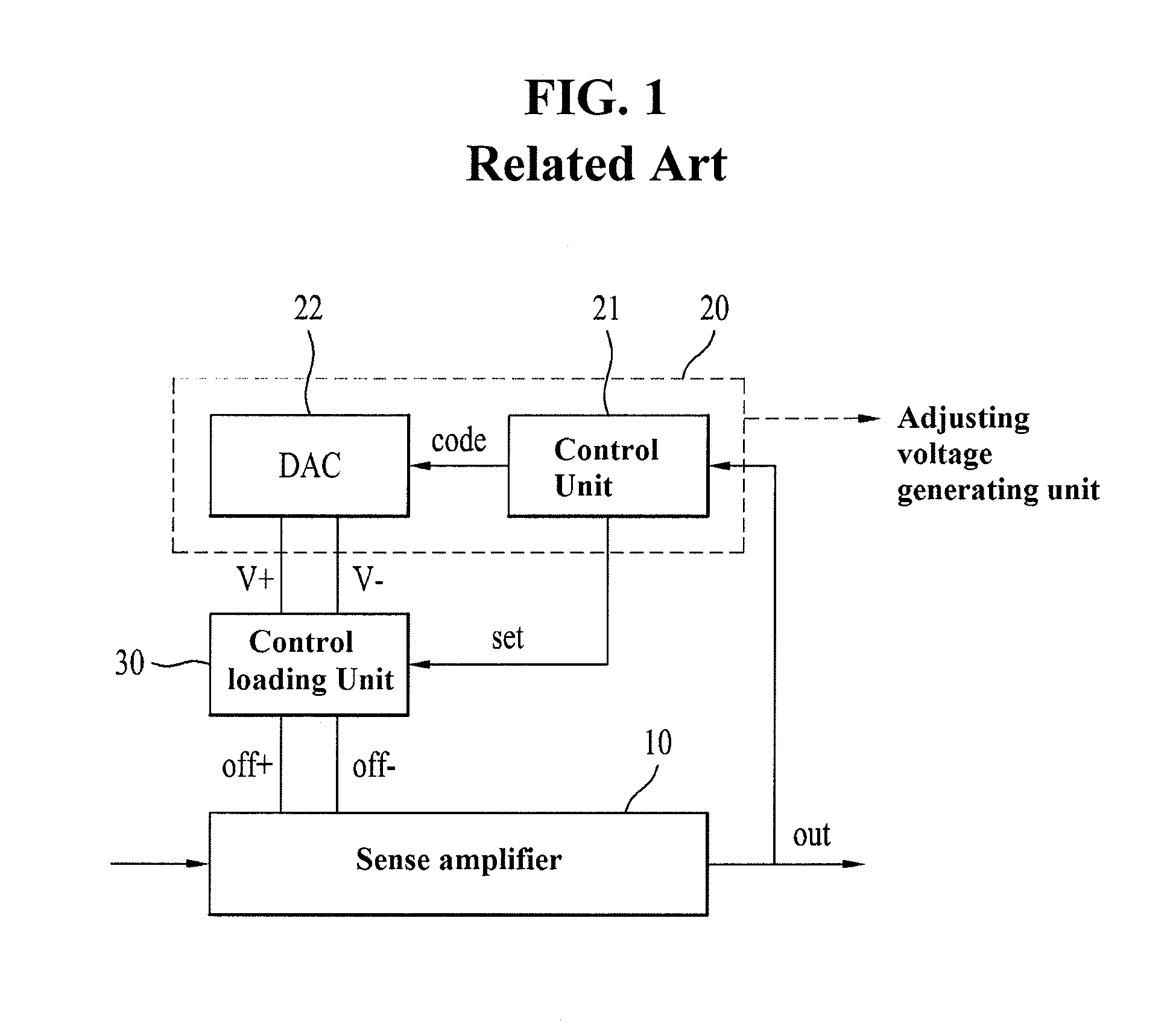
However, the related art offset adjusting circuit has the following problems.
That is, since the related art offset adjusting circuit has a structure in which the offset of the reference voltage on one digital-to-analog converter is corrected, in order to apply the related art offset adjusting circuit to a system having a plurality of the digital-to-analog converters, it is required to add the related art offset adjusting circuits as many as a number of the digital-to-analog converters, causing a problem in that a plurality of the reference voltages corresponding to the number of digital-to-analog converters must be controlled.

Method used


Image

  • Device and method for controlling reference voltage of digital-to-analog converter
  • Device and method for controlling reference voltage of digital-to-analog converter
  • Device and method for controlling reference voltage of digital-to-analog converter

Examples


Embodiment Construction

[0037]Reference will now be made in detail to the specific embodiments of the present invention, examples of which are illustrated in the accompanying drawings. Wherever possible, the same reference numbers will be used throughout the drawings to refer to the same or like parts.

[0038]FIG. 2 illustrates a block diagram of a device for controlling a reference voltage of a digital-to-analog converter in accordance with a preferred embodiment of the present invention, and FIG. 3 illustrates a block diagram of a test instrument in accordance with a preferred embodiment of the present invention.

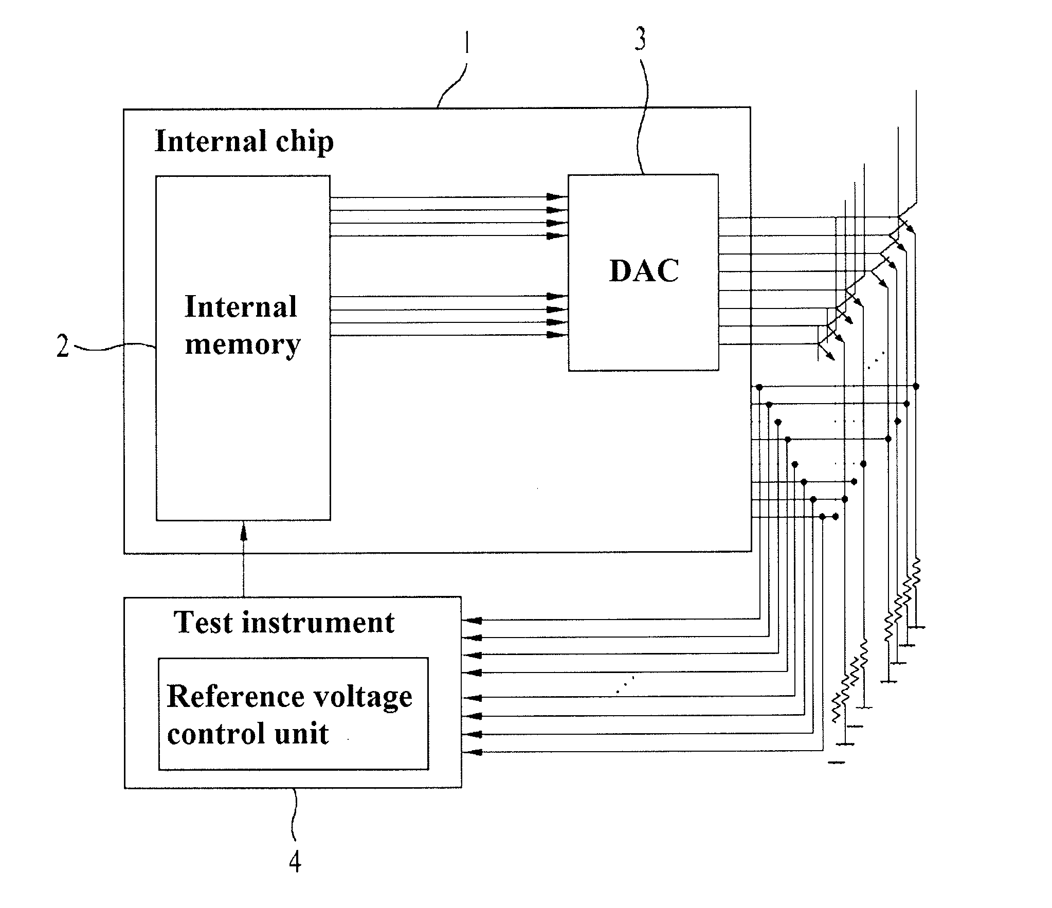
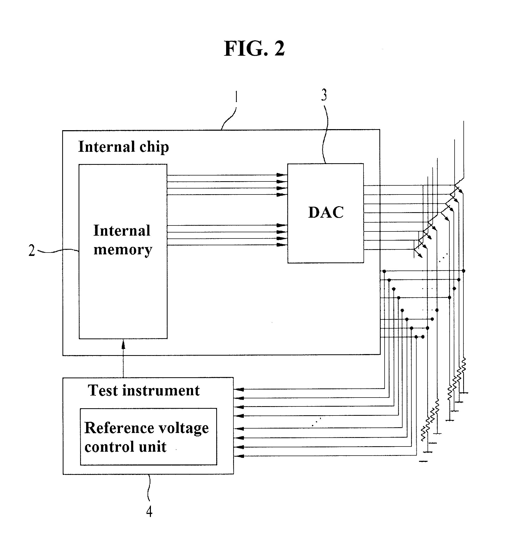
[0039]Referring to FIG. 2, the device for controlling a reference voltage of a digital-to-analog converter includes an internal chip 1 having an internal memory 2 and a DAC 3 for forwarding an analog voltage to each channel according to a preset reference voltage, and a test instrument 4 for measuring the voltage forwarded to each of the channels from the internal chip 1 to generate a code value wh...


PUM


Abstract

The present invention relates to device and method for controlling a reference voltage of a digital-to-analog converter for minimizing variation of output voltages among LED driving chips which drive an LED (Light Emitting Diode) backlight.

Description

CROSS REFERENCE TO RELATED APPLICATION[0001]This application claims the priority benefit of the Korean Patent Application No. 10-2010-0126914, filed on Dec. 13, 2010, which is hereby incorporated by reference as if fully set forth herein.BACKGROUND OF THE DISCLOSURE[0002]1. Field of the Disclosure[0003]The present invention relates to liquid crystal display devices, and more particularly to device and method for controlling a reference voltage of a digital-to-analog converter for minimizing variation of output voltages among LED driving chips which drive an LED (Light Emitting Diode) backlight.[0004]2. Discussion of the Related Art[0005]As information oriented society is developed, demands on image display devices increase in a variety of modes, and recently, many kinds of flat display devices, such as liquid crystal display devices, field emission display devices, plasma display panels, and light emitting display devices, are utilized.[0006]Among the flat display devices, the liqui...

Claims


Application Information

Patent Timeline
IPC IPC(8): H03M1/66
CPCH03M1/662H03M1/1038
Inventor SHIN, SUN-KYUNGJANG, CHUL-SANG
Owner LG DISPLAY CO LTD
Learn More