
Electrostatic chuck and method of manufacturing semiconductor device

a technology of electrostatic chuck and semiconductor device, which is applied in the direction of semiconductor/solid-state device manufacturing, basic electric elements, electric apparatus, etc., can solve the problems of difficult to move semiconductor chips and first substrates

Inactive Publication Date: 2012-05-31
SUMITOMO ELECTRIC IND LTD
View PDF3 Cites 165 Cited by
  • Summary
  • Abstract
  • Description
  • Claims
  • Application Information

AI Technical Summary

Benefits of technology

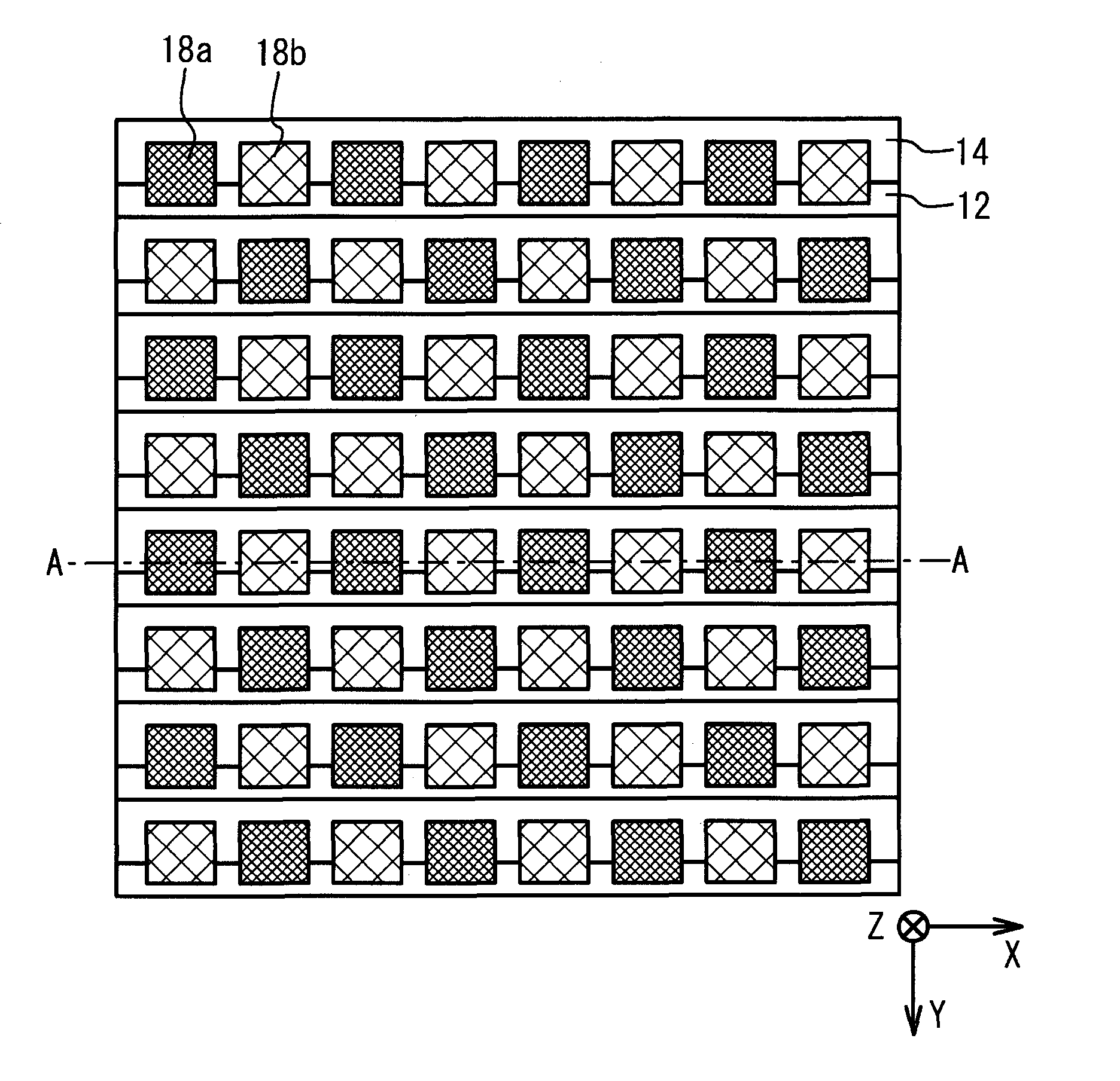
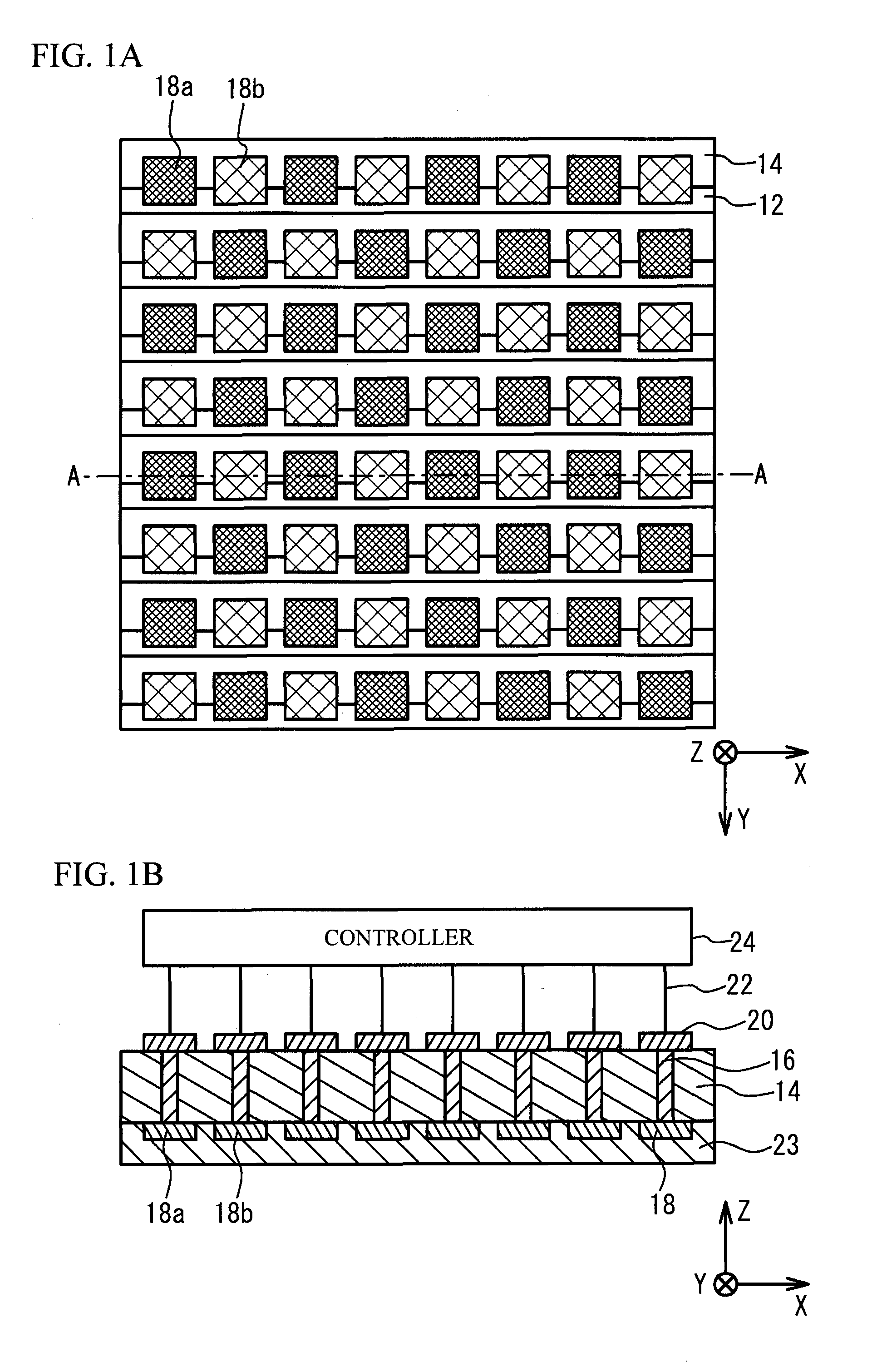
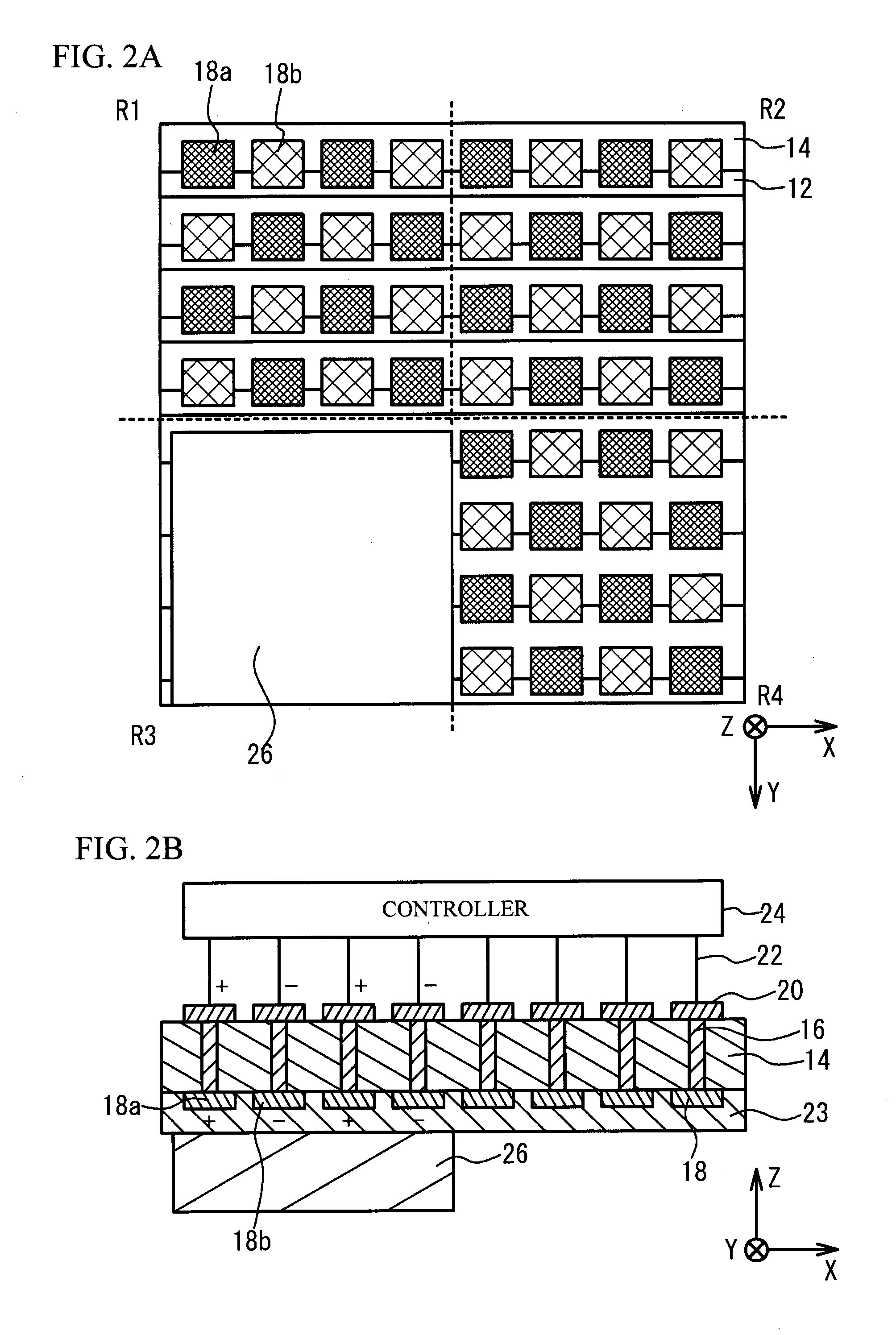
[0007]An area not operating as a device such as a pad area is not needed to be formed on an expensive substrate such as a single crystal SiC substrate. And so, it is thought that a semiconductor chip having a device area is formed on a first substrate, and the semiconductor chip is moved to a second substrate. However, it is not easy to move semiconductor chips arrayed on the first substrate at a first interval to the second substrate so as to be arrayed at a second interval.

Problems solved by technology

However, it is not easy to move semiconductor chips arrayed on the first substrate at a first interval to the second substrate so as to be arrayed at a second interval.

Method used


Image

  • Electrostatic chuck and method of manufacturing semiconductor device
  • Electrostatic chuck and method of manufacturing semiconductor device
  • Electrostatic chuck and method of manufacturing semiconductor device

Examples


second embodiment

[0054]A second embodiment is an example of a manufacturing method of a semiconductor device with use of the electrostatic chuck in accordance with the first embodiment. FIG. 11A through FIG. 18C illustrate a cross sectional view for explaining the manufacturing method of a semiconductor device in accordance with the second embodiment. As illustrated in FIG. 11A, a plurality of semiconductor elements 61 are formed on a substrate 50. The substrate 50 is, for example, a silicon substrate. The semiconductor element 61 is an FET (Field Effect Transistor) made of nitride semiconductor. An AlN layer 51 having a thickness of 0.1 μm is formed on the substrate 50. An undoped GaN layer 52 having a thickness of 2 μm is formed on the AlN layer 51. An AlGaN layer 53 (a composition ratio of Al is 0.25) having a thickness of 25 nm is formed on the GaN layer 52. The AlN layer 51, the undoped GaN layer 52 and the AlGaN layer 53 act as a semiconductor layer 58 and are formed with an MOVPE (Metal Organ...

third embodiment

[0087]A third embodiment is an example where different semiconductor chips are adhered to a substrate. FIG. 21A through FIG. 22 illustrate a plane view of a case where the semiconductor chip 60 is moved from the substrate 76 to the substrate 80. As illustrated in FIG. 21A, semiconductor chips 60d are arrayed on a substrate 76a at an interval P1d. As illustrated in FIG. 21B, semiconductor chips 60e are arrayed on a substrate 76b at an interval P1e. As illustrated in FIG. 21C, semiconductor chips 60f are arrayed on a substrate 76c at an interval P1f. The substrates 76a, 76b and 76c are a substrate including an electrostatic chuck as well as the substrate 76 of the second embodiment. The semiconductor chips 60d, 60e and 60f are, for example, an InP-based semiconductor element, a GaAs-based semiconductor element, a GaN-based semiconductor element respectively.

[0088]As illustrated in FIG. 21A, the pick-up device 78 picks-up the semiconductor chips 60d having the interval P2d on the subst...


PUM


Abstract

An electrostatic chuck device including: a plurality of adsorption areas having an electrode generating electrostatic attractive force; and a control portion controlling the electrostatic attractive force against each of the plurality of the adsorption areas independently of other adsorption areas.

Description

CROSS-REFERENCE TO RELATED APPLICATION[0001]This application is based upon and claims the benefit of priority of the prior Japanese Patent Application No. 2010-265790, filed on Nov. 29, 2010, the entire contents of which are incorporated herein by reference.BACKGROUND[0002](i) Technical Field[0003]The present invention relates to an electrostatic chuck and a method of manufacturing a semiconductor device.[0004](ii) Related Art[0005]For example, a nitride semiconductor device using a nitride semiconductor such as gallium nitride (GaN) is known as a high frequency and high output power device. Semiconductor layers of the nitride semiconductor device are formed on a SiC substrate or the like. A semiconductor chip having the nitride semiconductor device or the like has an area operating as a device and a pad area to be wire-bonded.[0006]Japanese Patent Application Publication No. 6-118441 and Japanese Patent Application Publication No. 6-167721 disclose a technology in which a semicondu...

Claims


Application Information

Patent Timeline
Patent Type & Authority Applications(United States)
IPC IPC(8): H01L21/687H01L21/50
CPCH01L21/6833
Inventor FURUYA, AKIRAKITAMURA, TAKAMITSU
Owner SUMITOMO ELECTRIC IND LTD
Learn More