Integrated semiconductor laser element, semiconductor laser module, and optical transmission system
a laser element and laser module technology, applied in the direction of semiconductor lasers, instruments, optical elements, etc., can solve the problem of increasing the deviation of the output intensity with respect to the wavelength, and achieve the effect of increasing the deviation of the output intensity
- Summary
- Abstract
- Description
- Claims
- Application Information
AI Technical Summary
Benefits of technology
Problems solved by technology
Method used
Image

Examples
first embodiment
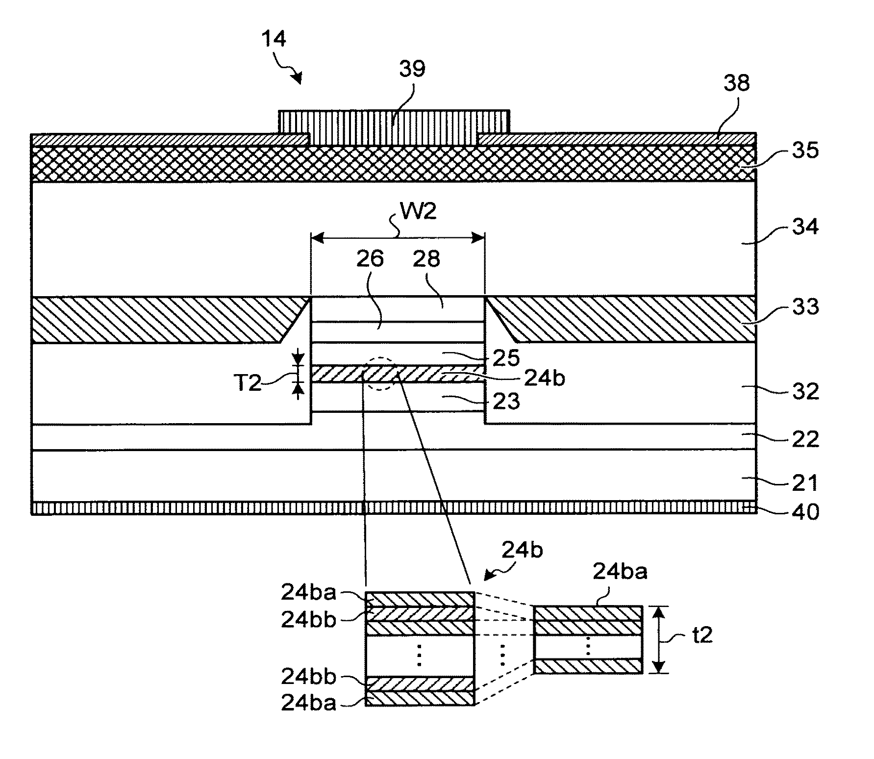
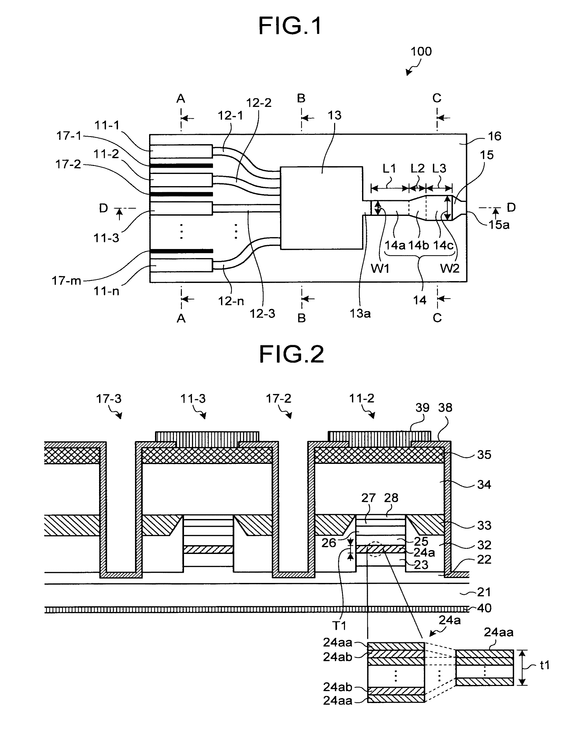
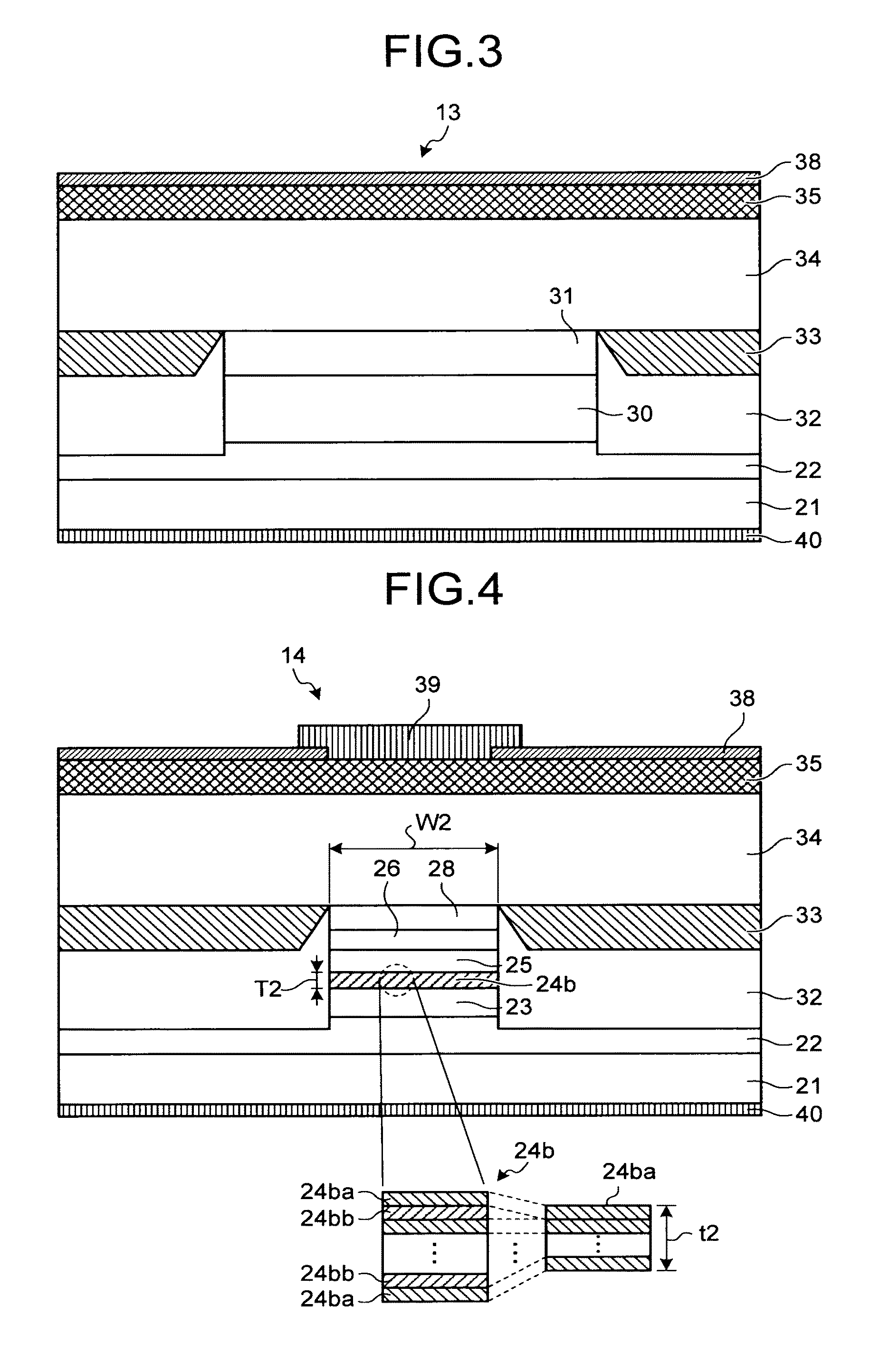
[0032]First, an integrated semiconductor laser element according to a first embodiment of the present invention is explained. FIG. 1 is a schematic plan view of the integrated semiconductor laser element according to the first embodiment.
[0033]As shown in FIG. 1, an integrated semiconductor laser element 100 according to the first embodiment includes a plurality of DFB lasers 11-1 to 11-n (n is an integer equal to or larger than 2) each having a mesa structure, a plurality of optical waveguides 12-1 to 12-n, an optical coupler 13, a semiconductor optical amplifier 14, and a spot size converter 15, constituting a structure in which all these constituent elements are integrated on a single semiconductor substrate and then embedded by an embedding portion 16. Furthermore, in the embedding portion 16 between the DFB lasers 11-1 to 11-n, trench grooves 17-1 to 17-m (m=n−1) are provided. An outline of each of the constituent elements, such as the DFB lasers 11-1 to 11-n shown in FIG. 1, i...
example 1
[0054]Subsequently, as an Example 1, the integrated semiconductor laser element according to the first embodiment shown in FIG. 1 was manufactured. In the integrated semiconductor laser element according to the Example 1, as for the width of the active layer of the semiconductor optical amplifier, the width of the equal width portion is 1.5 μm, and the width of the expanded width portion is 4.0 μm. Furthermore, as for the length, the length of the equal width portion is 450 μm, the length of the tapered portion is 343 μm, and the length of the expanded width portion is 122 μm. The thickness of each of the well layers of the active layer of the DFB laser and the semiconductor optical amplifier is 6 nm, and the number of the well layers is seven. Therefore, the total volume of the well layers of the active layer of the semiconductor optical amplifier is 92.064 μm3. The composition of each of the well layers is set such that the gain peak of the semiconductor laser is positioned on a s...
example 2
[0056]Subsequently, as an Example 2, an integrated semiconductor laser element was manufactured with a thickness of the well layer of the active layer different from that of the Example 2. In the integrated semiconductor laser element according to the Example 2, the widths of the equal width portion and the expanded width portion and the lengths of the equal width portion, the tapered portion, and the expanded width portion of the active layer of the semiconductor optical amplifier are the same as those of the Example 1. The thickness of each of the well layers of the active layer of the DFB laser and the semiconductor optical amplifier is 7 nm, and the number of the well layers is seven. Therefore, the total volume of the well layers of the active layer of the semiconductor optical amplifier is 107.408 μm3. The composition of each of the well layers is set such that the gain peak is positioned near the center of the wavelength band that is formed with the oscillation wavelengths of...
PUM
 Abstract
Description
Claims
Application Information
 - R&D
- Intellectual Property
- Life Sciences
- Materials
- Tech Scout
- Unparalleled Data Quality
- Higher Quality Content
- 60% Fewer Hallucinations
Browse by: Latest US Patents, China's latest patents, Technical Efficacy Thesaurus, Application Domain, Technology Topic, Popular Technical Reports.
© 2025 PatSnap. All rights reserved.Legal|Privacy policy|Modern Slavery Act Transparency Statement|Sitemap|About US| Contact US: help@patsnap.com