Thin film transistors and methods for manufacturing the same

a technology of thin film transistors and transistors, which is applied in the direction of semiconductor devices, semiconductor/solid-state device details, electrical equipment, etc., can solve the problems of reducing plasma, etching stop layer needs an additional photomask, and device breakage of reducing plasma

Active Publication Date: 2012-05-17
INNOLUX CORP
View PDF1 Cites 29 Cited by
  • Summary
  • Abstract
  • Description
  • Claims
  • Application Information

AI Technical Summary

Problems solved by technology

However, the process utilizing the etching stop layer needs an additional photomask.
The oxide semiconductor is sensitive to the plasma of reducing atmosphere, and the reducing plasma may break a device made thereby.

Method used


Image

  • Thin film transistors and methods for manufacturing the same
  • Thin film transistors and methods for manufacturing the same
  • Thin film transistors and methods for manufacturing the same

Examples


Embodiment Construction

[0013]The following description is of the best-contemplated mode of carrying out the invention. This description is made for the purpose of illustrating the general principles of the invention and should not be taken in a limiting sense. The scope of the invention is best determined by reference to the appended claims.

[0014]The making and using of the TFTs in the embodiments of the disclosure are discussed in detail below. It should be appreciated, however, that the embodiments provide many applicable inventive concepts that can be embodied in a wide variety of specific contexts. The specific embodiments discussed are merely illustrative, and do not limit the scope of the disclosure.

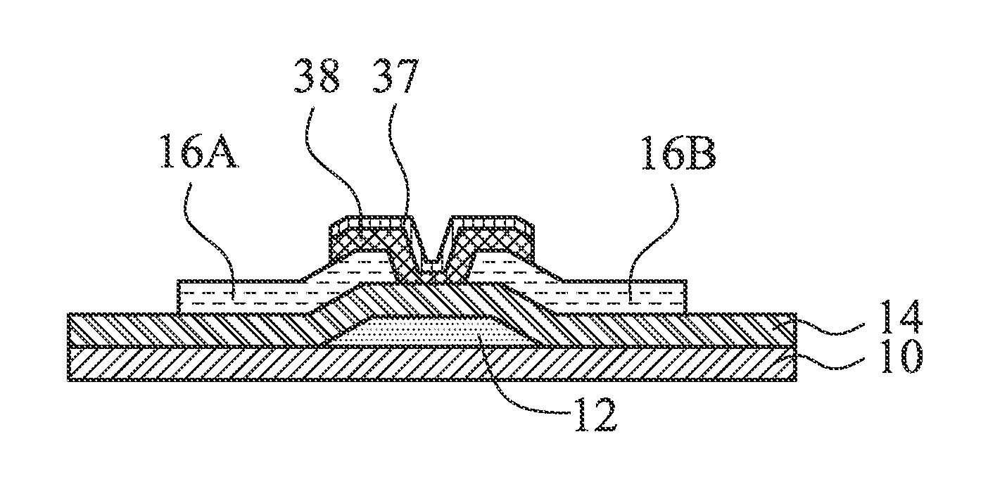
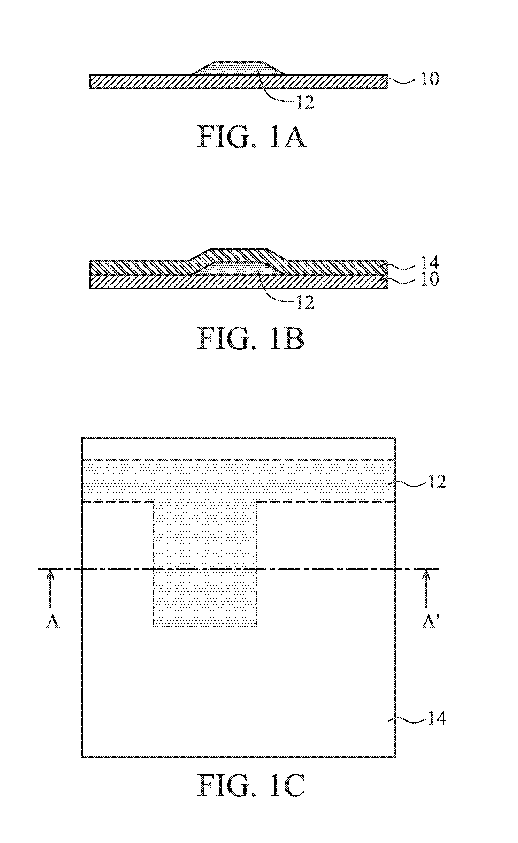
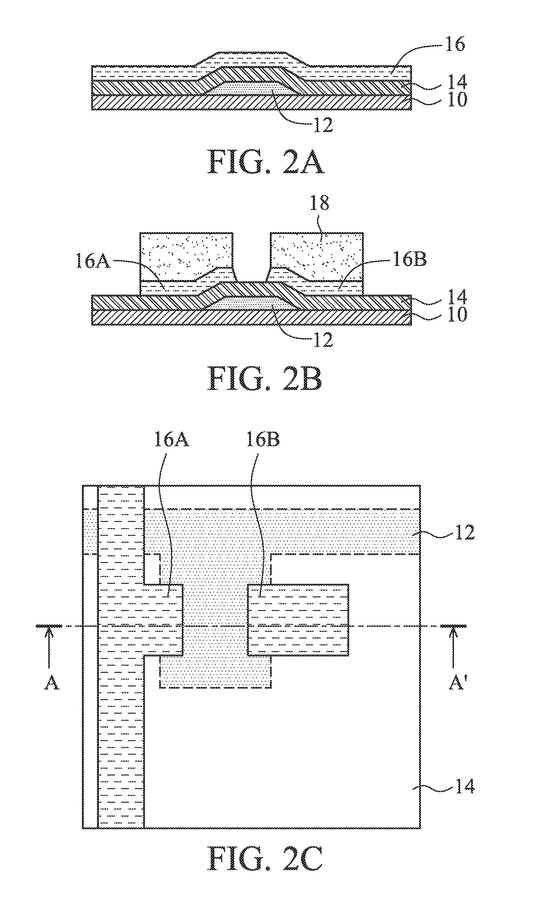
[0015]As shown in FIG. 1A, a patterned metal layer 12 is formed on a substrate 10. The substrate 10 comprises rigid inorganic material such as transparent material (e.g. glass, quartz, and the likes) or opaque material (e.g. wafer, ceramic, and the likes), or flexible organic material (e.g. plastic, rubb...


PUM

PropertyMeasurementUnit
widthaaaaaaaaaa
widthaaaaaaaaaa
semiconductoraaaaaaaaaa

Abstract

Disclosed is a thin film transistor including a gate electrode on a substrate. A gate dielectric layer is disposed on the gate electrode and the substrate, and source/drain electrodes are disposed on the gate dielectric layer overlying two edge parts of the gate electrode. A channel layer is disposed on the gate dielectric layer overlying a center part of the gate electrode, and the channel region contacts the source/drain electrodes. An insulating capping layer overlies the channel layer, wherein the channel layer includes an oxide semiconductor.

Description

CROSS REFERENCE TO RELATED APPLICATIONS[0001]This Application claims priority of Taiwan Patent Application No. 99139500, filed on Nov. 17, 2010, the entirety of which is incorporated by reference herein.BACKGROUND OF THE INVENTION[0002]1. Field of the Invention[0003]The present invention relates to thin film transistors, and in particular relates to methods and structures of utilizing an oxide semiconductor as channel layers of the thin film transistors.[0004]2. Description of the Related Art[0005]In the process of forming thin film transistors (TFT), oxide semiconductors have become a main trend for related industries in Japan and Korea. The oxide semiconductors can be zinc oxide (ZnO), gallium-doped zinc oxide (GZO), aluminum zinc oxide (AZO), zinc tin oxide (ZTO), indium zinc oxide (IZO), and indium gallium zinc oxide (IGZO), and the likes. The oxide semiconductor process may adopt a five photomask process such as a back channel etching (BCE) process or a coplanar process for an ...

Claims


Application Information

Patent Timeline
Patent Type & Authority Applications(United States)
IPC IPC(8): H01L29/786H01L21/336
CPCH01L29/66742H01L29/786H01L29/78606H01L29/66969H01L2924/0002H01L29/7869H01L2924/00H01L27/1225H01L23/3171H01L23/481H01L29/41733H01L29/41775H01L29/517H01L29/518H01L21/441H01L21/47H01L21/471H01L21/47573H01L27/1259
Inventor LIN, HSIN-HUNGCHANG, JUNG-FANGKAO, KER-YIH
Owner INNOLUX CORP
Why Eureka
Try Eureka