Data processing method and semiconductor integrated circuit

a data processing and semiconductor technology, applied in the field of data processing methods and semiconductor integrated circuits, can solve the problems of difficult to increase data read reliability and another block with a lower degree of reliability, and achieve the effects of reducing the faulty operation of the semiconductor device, accurate reconstruction, and increasing data read reliability

Inactive Publication Date: 2012-04-19
PANASONIC CORP
View PDF2 Cites 2 Cited by
  • Summary
  • Abstract
  • Description
  • Claims
  • Application Information

AI Technical Summary

Benefits of technology

[0006]Thus, it is an objective of the technique disclosed in this specification to provide a method for reading data with a high degree of data read reliability and a semiconductor integrated circuit.
[0014]A semiconductor integrated circuit according to another aspect of the present invention is A semiconductor integrated circuit for sequentially processing a data string stored in a flash memory on a block-by-block basis, the semiconductor integrated circuit including: a CPU; and a RAM, wherein the flash memory includes p designated blocks, where p≧2, and ordinary block groups, each of the ordinary block groups includes p ordinary blocks, p divided data strings obtained by dividing the data string into p strings are stored in the p designated blocks, respectively, the p divided data strings stored in the p designated blocks are respectively copied to the p ordinary blocks included in each of the ordinary block groups, reliability of the designated blocks is higher than reliability of the ordinary blocks, the CPU executes a read process on an ith designated block storing an ith divided data string, where 1≦i≦n, the CPU sequentially executes the read process on ith ordinary blocks each of which stores the ith divided data string and which are respectively included in the ordinary block groups if the ith divided data string is not normally read from the ith designated block, the CPU transfers the ith divided data string normally read from any one of the ith designated block or the ith ordinary blocks to the RAM, the CPU determines whether or not reading the p divided data strings has been completed if the ith divided data string is normally read from any one of the ith designated block or the ith ordinary blocks, and the CPU executes the read process on an (i+1)th designated block storing an (i+1)th divided data string following the ith divided data string if the CPU determines that the reading the p divided data strings has not been completed. In the semiconductor integrated circuit, a designated block having a high degree of reliability than an ordinary block is preferentially selected as a block on which a read process is performed, so that it is possible to increase data read reliability (the probability that a normal divided data string can be read).

Problems solved by technology

However, in the semiconductor device of Patent Document 1, a designated block is not always preferentially selected as a target of a read process, and another block with a lower degree of reliability than the designated block may be continuously selected as the target of the read process.
Thus, it has been difficult to increase data read reliability (the probability that normal data can be read).
Note that a similar problem also arises when the NAND type flash memory stores a data string other than the boot program.

Method used


Image

  • Data processing method and semiconductor integrated circuit
  • Data processing method and semiconductor integrated circuit
  • Data processing method and semiconductor integrated circuit

Examples


first embodiment

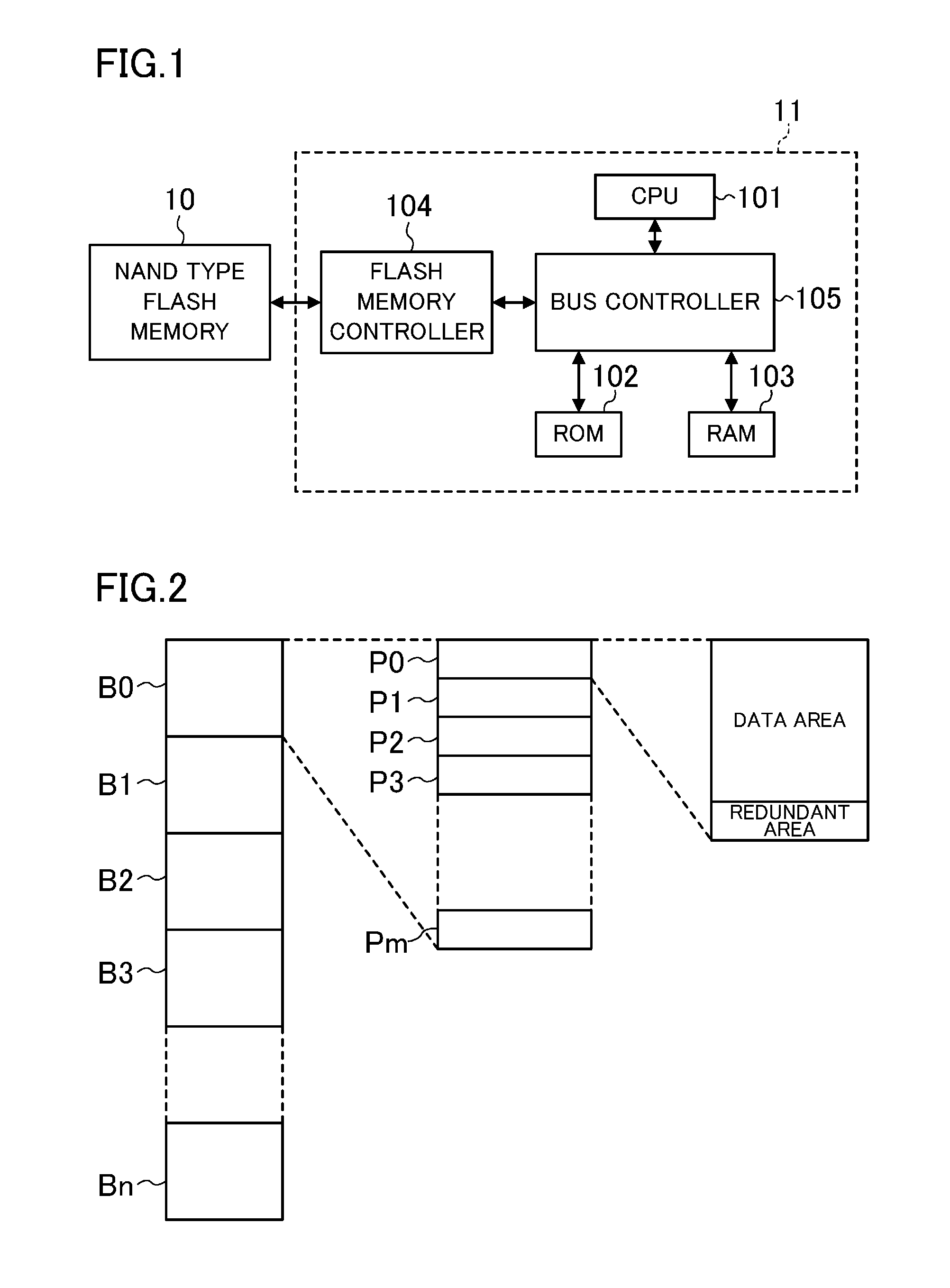
[0032]FIG. 1 illustrates an example configuration of a semiconductor device according to a first embodiment. The semiconductor device includes a NAND type flash memory 10, and a system LSI 11 (semiconductor integrated circuit). The NAND type flash memory 10 is provided outside the system LSI 11. The system LSI 11 includes a variety of circuits integrated on a single semiconductor chip.

[0033][NAND Type Flash Memory]

[0034]The NAND type flash memory 10 stores a variety of processing programs and data including a boot program to activate the semiconductor device.

[0035]As illustrated in FIG. 2, the NAND type flash memory 10 includes a plurality of blocks B0, B1, . . . , Bn (n≧2). Each of the blocks B0, B1, . . . , Bn includes a plurality of pages P0, P1, . . . , Pm (m≧2). Unique block numbers (0, 1, . . . , n) are assigned to the blocks B0, B1, . . . , Bn, respectively. Unique page numbers (0, 1, . . . , m) are assigned to the pages P0, P1, . . . , Pm, respectively. In accessing the NAND...

second embodiment

[0090]FIG. 6 illustrates an example configuration of a semiconductor device of a second embodiment. The semiconductor device has the configuration of the semiconductor device illustrated in FIG. 1, and in addition, a non-volatile memory 20. Note that the non-volatile memory 20 may be provided inside the system LSI 11 or may be provided outside the system LSI.

[0091]In the course of using the NAND type flash memory 10, the number of unreadable blocks in the NAND type flash memory 10 randomly increases. Thus, when access to the NAND type flash memory 10 is performed without the unreadable blocks being avoided, the start-up time of the semiconductor device may increase as the number of unreadable blocks increases. The semiconductor device illustrated in FIG. 6 performs the process of storing boot history information (information indicating from which blocks the divided programs D1, D2, D3 have been able to be normally read) in the non-volatile memory 20, and the process of sequentially ...

third embodiment

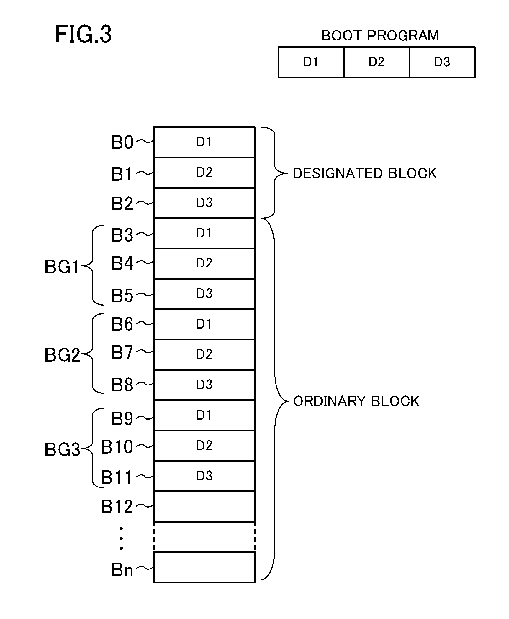
[0110]FIG. 11 illustrates an example configuration of a semiconductor device of a third embodiment. The semiconductor device includes a system LSI 31 instead of the system LSI 11 illustrated in FIG. 6. The system LSI 31 has the configuration of the system LSI 11 illustrated in FIG. 1, and in addition, a block copy determination circuit 301. For example, the block copy determination circuit 301 compares the number of unreadable blocks of each of the divided programs D1, D2, D3 with a preset threshold value, and outputs a copy request signal (signal to request that each of the divided programs D1, D2, D3 is copied to an unused block).

[0111]For example, in the NAND type flash memory 10, as illustrated in FIG. 7, when three of four blocks (the designated block B2 and the ordinary blocks B5, B8, B11) each storing the divided program D3 are unreadable blocks, the divided program D3 cannot be normally read if the ordinary block B11 becomes an unreadable block, so that the boot program cann...


PUM


Abstract

A read process is performed on an ith designated block storing an ith divided data string. If the ith divided data string is not normally read, the read process is sequentially executed on ith ordinary blocks each storing the ith divided data string, where the ith ordinary blocks are included in ordinary block groups, respectively. When the ith divided data string is normally read, it is determined whether or not reading p divided data strings has been completed. If it is determined that the reading the p divided data strings has not been completed, the read process is performed on an (i+1)th designated block storing an (i+1)th divided data string following the ith divided data string.

Description

CROSS-REFERENCE TO RELATED APPLICATION[0001]This is a continuation of PCT International Application PCT / JP2009 / 006753 filed on Dec. 10, 2009, which claims priority to Japanese Patent Application No. 2009-155170 filed on Jun. 30, 2009. The disclosures of these applications including the specifications, the drawings, and the claims are hereby incorporated by reference in their entirety.BACKGROUND[0002]The technology disclosed in this specification relates to methods for sequentially processing data strings in flash memories on a block-by-block basis, and to semiconductor integrated circuits, specifically to improvement of data read reliability (the probability that normal data can be read).[0003]In recent years, system LSIs including a large number of functions integrated on one chip are used in various electronic devices. Moreover, non-volatile memories which store various processing programs such as a boot program and data are provided inside or outside the system LSIs. As such non-...

Claims


Application Information

Patent Timeline
Patent Type & Authority Applications(United States)
IPC IPC(8): G06F12/02G06F11/10H03M13/05
CPCG06F11/1068G06F11/1402G06F2212/7202G06F12/0246G06F11/1417
Inventor TAKAHASHI, TSUKASASEZAKI, TOMOHISATSUBOI, NOBUHIROMINO, YOSHITERU
Owner PANASONIC CORP
Why Eureka
Try Eureka