
Schottky-barrier junction element, and photoelectric conversion element and solar cell using the same

a photoelectric conversion element and junction element technology, applied in the direction of electrical apparatus, solid-state devices, semiconductor devices, etc., can solve the problems of difficult practical use, limited sensitivity of wavelength region allowing elements to have photoelectric conversion elements less than 380 nm, etc., to achieve effective use of photoelectric effect in visible light range, high light transmittance, and good performance

Inactive Publication Date: 2012-03-22
NAT INST FOR MATERIALS SCI
View PDF2 Cites 2 Cited by
  • Summary
  • Abstract
  • Description
  • Claims
  • Application Information

AI Technical Summary

Benefits of technology

[0017]According to the present invention, by providing an organic conductor on a specific inorganic semiconductor, a Schottky-barrier junction element having a high Schottky barrier can be provided. In particular, since the organic conductor has high light transmittance, the use as a photoelectric conversion element and solar cell exhibits good performance. By selecting an inorganic semiconductor having a specific band gap, absorption wavelength can be shifted from ultraviolet light to visible light, which ensures effective use of photoelectric effect in the visible light range.

Problems solved by technology

With the conventional Schottky-barrier photoelectric conversion elements such as the one disclosed in Non-patent Literature 1, since significant attenuation of incident light occurs at metallic thin film electrodes, sufficient performance as a photoelectric conversion element cannot be ensured, which makes it difficult to put it into practical use.
However, since Shottky-barrier photoelectric conversion elements use oxides having a large optical band gap such as TiO2 and SrTiO3 as semiconductors, the wavelength region allowing the elements to have sensitivity as photoelectric conversion elements has been limited to shorter than 380 nm.

Method used


Image

  • Schottky-barrier junction element, and photoelectric conversion element and solar cell using the same
  • Schottky-barrier junction element, and photoelectric conversion element and solar cell using the same
  • Schottky-barrier junction element, and photoelectric conversion element and solar cell using the same

Examples


example 1

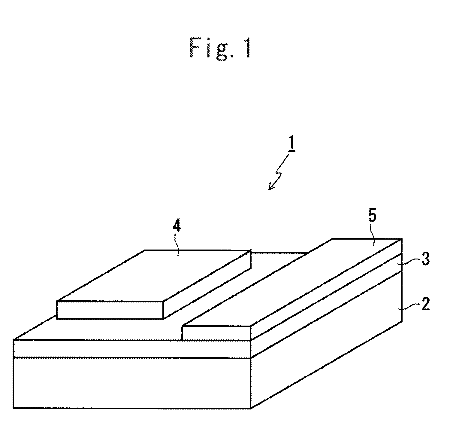
[0045]A solar cell having the same structure as the one shown in FIG. 1 was made. The solar cell will be described by referring to FIG. 1. The solar cell 1 of this example includes a sapphire substrate 2, a GaN film 3 provided on the substrate, and an organic conductor (ORMECON) 4 and an indium electrode 5 aligned on the GaN film 3.

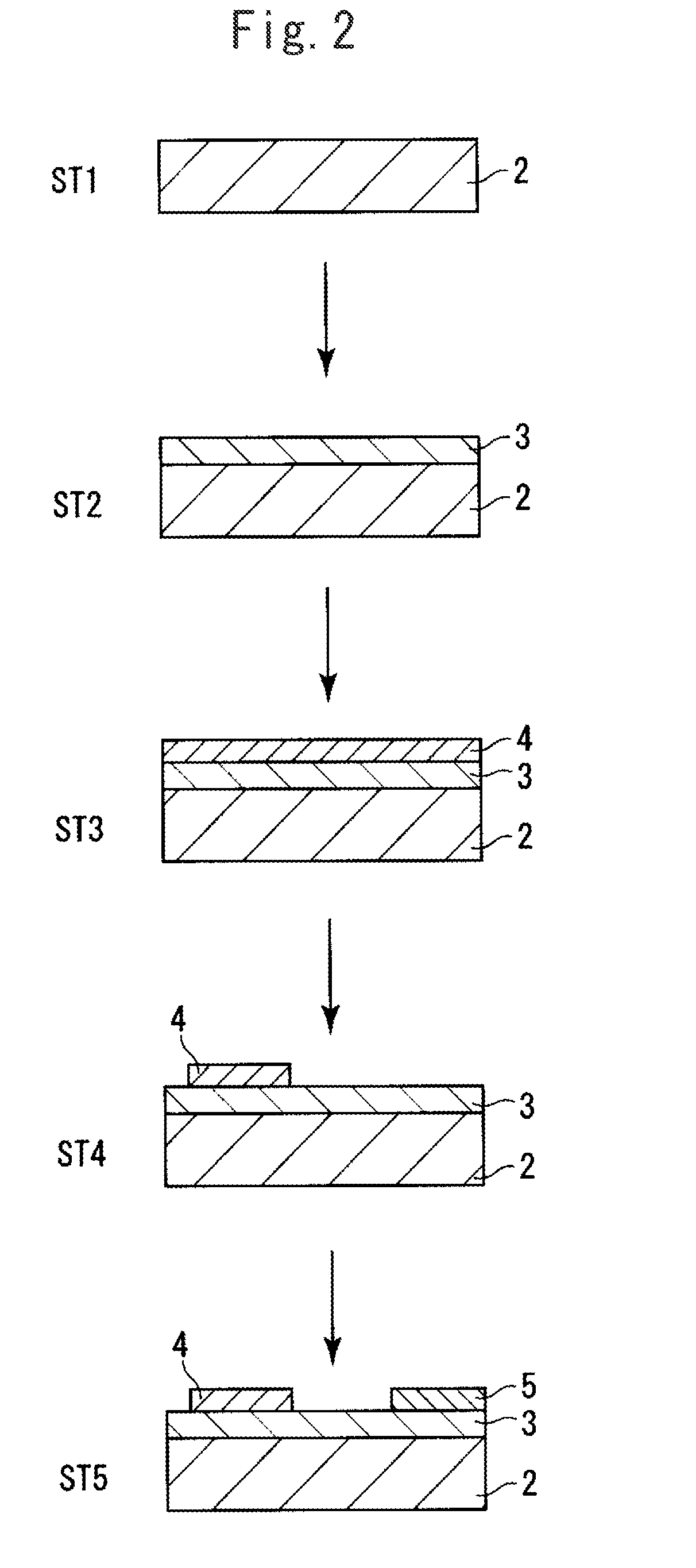
[0046]FIG. 2 shows the flow of manufacturing the solar cell shown in FIG. 1.

[0047]In step ST1, a sapphire (0001) substrate 2 was prepared. In step ST2, using trimethyl gallium, ammonia, and hydrogen as raw materials, epitaxial growth of gallium nitride (GaN) was promoted by the organic metal vapor phase growth method until a thickness of 3 μm was obtained to form a GaN film 3 on the sapphire (0001) substrate 2. In Example 1, a commercially available sapphire substrate 2 having a GaN film 3 on its surface was used. This sapphire substrate 2 was n-GaN epitaxial wafer (wafer No. PT01AB04H26491121) (POWDEC K.K.) with an undoped layer having the thickness of 1...

example 2

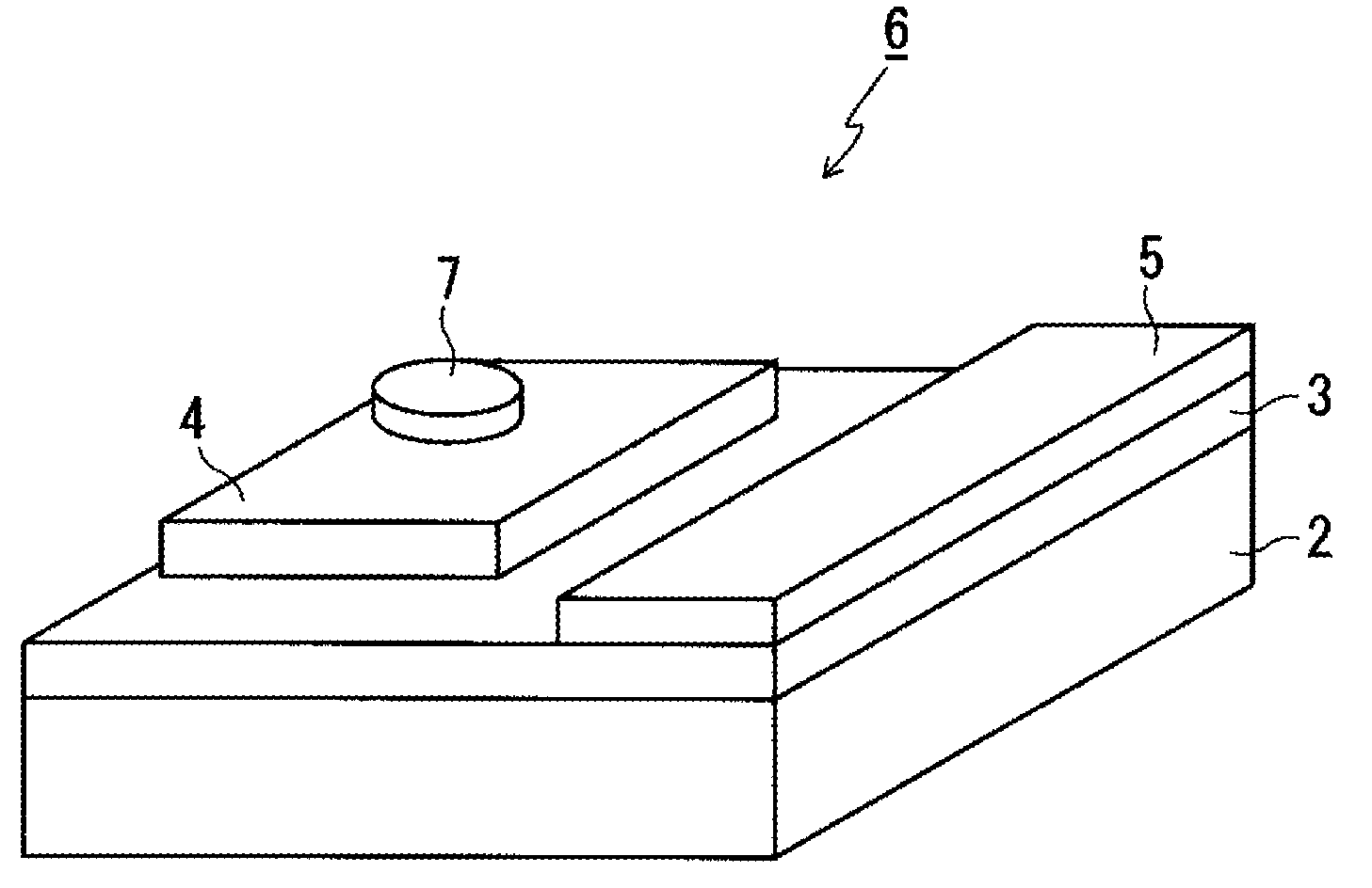
[0057]FIG. 7 is a perspective view illustrating the structure of a solar cell 6 related to Example 2. The solar cell 6 is structured with a transparent conductive oxide 7, organic conductor 4, and inorganic semiconductor 3 interfaced together. The solar cell 6 includes: a sapphire substrate 2; a GaN film as an inorganic semiconductor 3 provided on the sapphire substrate 2; ORMECON (highly-conductive polyaniline-series organic solvent solution) as the organic conductor 4 and an indium electrode 5 aligned on the inorganic semiconductor 3; and a transparent conductive oxide 7 provided on the surface of the organic conductor 4.

[0058]FIG. 8 illustrates the manufacturing process of the solar cell 6 shown in FIG. 7.

[0059]In step ST6, a sapphire substrate 2 was provided, in step 7, a GaN film was formed on the sapphire substrate 2 as the inorganic semiconductor 3, and in step 8, an organic conductor 4 was formed on the GaN film as the inorganic semiconductor 3, all of which are the same as ...

example 3

[0067]As Example 3, an element was made following the same procedure as Example 1, with a non-doped GaN film having the thickness of 1 μm used as the inorganic semiconductor 3, PEDOT:PSS having the thickness of 10 μm as the organic conductor 4, and an Ag film having the thickness of 100 μm as the electrodes 5.

[0068]Similar to Example 1, the current / voltage characteristics were measured to calculate the current density / voltage characteristics. With the element manufactured in Example 3, the ideal diode value n was 1.8, ideal saturated current density J0 was 6.5×10⁻¹² A, and the Schottky barrier height fB was 1.8 eV.

[0069]Similar to Example 1, current / voltage measurement was conducted while the light of the xenon lamp was irradiated, and the voltage at open end VOC, short-circuit current Isc, maximum output Pmax, and fill factor FF were found to be 0.44 V, 3.84 nA, 0.64 nW, and 0.38 respectively.

[0070]Table 2 summarizes the results of Example 1 to Example 3.

TABLE 2Example 1Example 2Ex...


PUM


Abstract

A Schottky-barrier junction element 1 has a Schottky-barrier junction between an organic semiconductor 3 and an organic conductor 4. The inorganic semiconductor 3 is any one of nitride semiconductors, Si, GaAs, CdS, CdTe, CuInGaSe, InSb, PbTe, PbS, Ge, InN, GaSb, and SiC. A solar cell uses this Schottky-barrier junction element 1, with its photoelectric conversion section including the Schottky junction. A photoelectric conversion element uses this Schottky-barrier junction element 1, with its conversion section for interconverting light and electricity including the Schottky junction.

Description

TECHNICAL FIELD [0001]The present invention relates to a Schottky-barrier junction element having a Schottky-barrier junction formed between an inorganic semiconductor and an organic conductor, and a photoelectric conversion element and a solar cell using the same.BACKGROUND ART [0002]A Schottky-barrier junction between a metal and a semiconductor is known. This Schottky-barrier junction is used in Si integrated circuits in combination with bipolar transistors and field-effect transistors.[0003]Non-patent Literature 1 discloses a Schottky-barrier photoelectric conversion element wherein a Schottky barrier is formed between an n-type semiconductor and a metallic thin film having work function of 5 eV or higher such as Au and Pd. With the conventional Schottky-barrier photoelectric conversion elements such as the one disclosed in Non-patent Literature 1, since significant attenuation of incident light occurs at metallic thin film electrodes, sufficient performance as a photoelectric c...

Claims


Application Information

Patent Timeline
Patent Type & Authority Applications(United States)
IPC IPC(8): H01L31/07H01L29/161H01L29/47H01L29/20
CPCY02E10/549H01L51/4213H10K30/10H10K30/50H01L31/07H01L31/108H01L31/04
Inventor MATSUKI, NOBUYUKIIROKAWA, YOSHIHIROITAKA, KENJIKOINUMA, HIDEOMISUMIYA, MASATOMO
Owner NAT INST FOR MATERIALS SCI
Learn More