
Method of Forming Conformal Film Having Si-N Bonds on High-Aspect Ratio Pattern

a technology of conformal film and high-aspect ratio, applied in the direction of coating, chemical vapor deposition coating, plasma technique, etc., can solve the problems of poor conformality or poor step coverage on a substrate containing small and/or high aspect ratio features, poor conformal coverage can hamper the development of higher density circuit devices and elements, etc., to improve the conformality or step coverage of the film, increase the mobility and diffusivity of molecules on the surface, and improve the effect of conformality

Active Publication Date: 2012-03-08
ASM JAPAN
View PDF2 Cites 78 Cited by
  • Summary
  • Abstract
  • Description
  • Claims
  • Application Information

AI Technical Summary

Benefits of technology

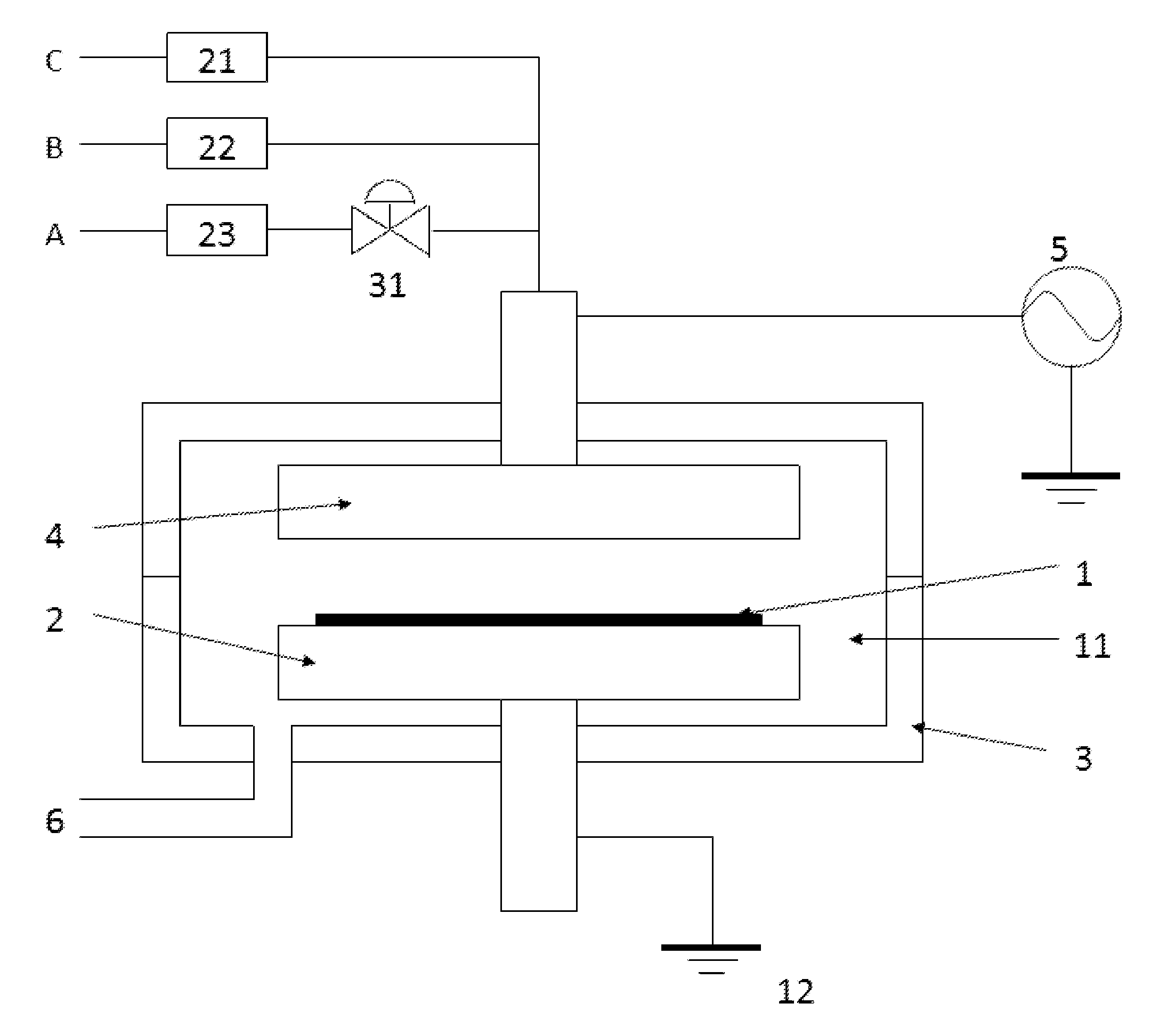
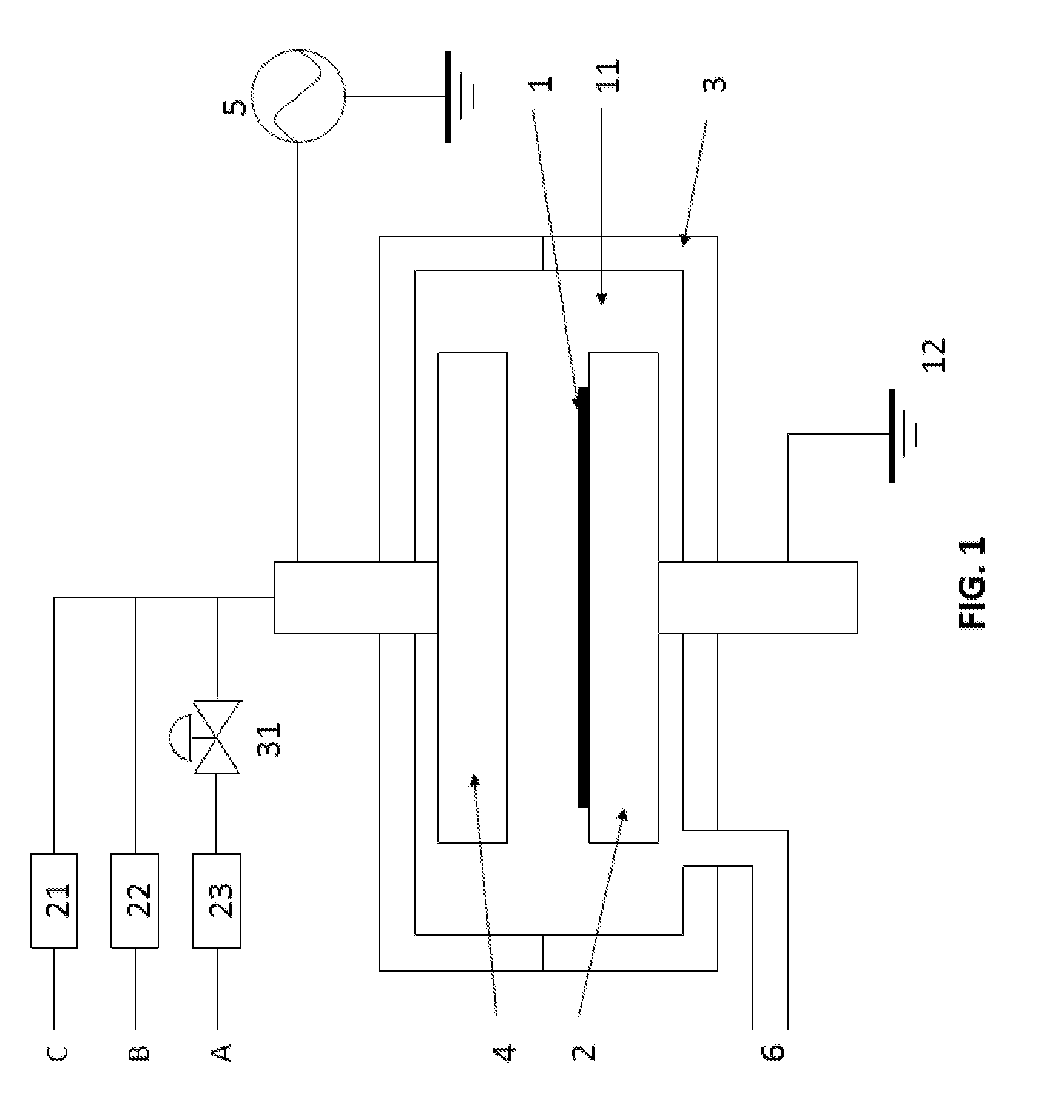
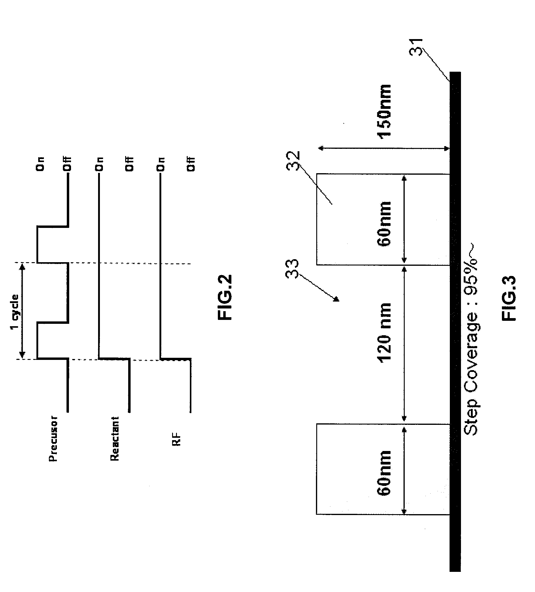
[0010]In some embodiments, RF plasma is generated by two-step application of RF power in pulses, while being synchronized with pulses of a silicon precursor. The first application takes place during the period of introducing the silicon precursor. In some embodiments, during the first application, RF plasma is generated after the introduction of the silicon precursor begins by delayed application of first RF power. In some embodiments, the intensity of the first RF power is low and / or the duration of the first RF power is short so as to decompose the precursor and make its molecules adsorb on the surface of the substrate, without increasing mobility and diffusivity of the molecules on the surface. The second application takes place during the period of introducing no silicon precursor. In some embodiments, during the second application, RF plasma is generated by applying second RF power at an intensity higher than that of the first RF power and / or for a period shorter than that of the first RF power so as to increase mobility and diffusivity of the molecules. In other words, in some embodiments, the first step of RF plasma is for generating and adsorbing molecules of silicon precursor on the surface, whereas the second step of RF plasma is for migrating the molecules on the surface, thereby improving the conformality or step coverage of a film.

Problems solved by technology

However, the PECVD method for forming silicon nitride leads to poor conformality or poor step coverage on a substrate containing small and / or high aspect ratio features.
In small circuits and devices, such as ultra-large scale integrated (ULSI) circuitry, poor conformal coverage can hamper the development of higher density circuit devices and elements.

Method used


Image

  • Method of Forming Conformal Film Having Si-N Bonds on High-Aspect Ratio Pattern
  • Method of Forming Conformal Film Having Si-N Bonds on High-Aspect Ratio Pattern
  • Method of Forming Conformal Film Having Si-N Bonds on High-Aspect Ratio Pattern

Examples


example 3

[0081]Under the same conditions as in Example 1, except for the pressure, a SiCN layer was formed on the substrate with the trenches having an aspect ratio of 2.5. The pressure was 600 Pa. After completion of the deposition, the trenches were observed with a scanning electron microscope (SEM) and the conformality was determined.

[0082]The results are shown in Table 2 below.

TABLE 2ConformalityPressure (Pa)300 (Example 1)600 (Example 3)Conformality95%89%

[0083]As shown in Table 2, in Example 3, when the pressure was higher (Example 3), the conformality was not as good as that when the pressure was low (Example 1). However, the conformality in Example 3 was significantly superior to that in Comparative Example 1 since the RF power was applied in two steps as in Example 1.

[0084]A significant advantage of the method of at least one of the disclosed embodiments of the present invention is that highly-conformal silicon nitride layers or other Si—N dielectric layers can be formed on various t...


PUM

PropertyMeasurementUnit
Fractionaaaaaaaaaa
Timeaaaaaaaaaa
Timeaaaaaaaaaa

Abstract

A method of forming a conformal dielectric film having Si—N bonds on a substrate having a patterned surface includes: introducing a reactant gas into a reaction space; introducing a silicon precursor in pulses of less than 5-second duration into the reaction space; applying a first RF power to the reaction space during the pulse of the silicon precursor; applying a second RF power to the reaction space during the interval of the silicon precursor pulse, wherein an average intensity of the second RF power during the interval of the silicon precursor pulse is greater than that of the first RF power during the pulse of the silicon precursor; and repeating the cycle to form a conformal dielectric film having Si—N bonds with a desired thickness on the patterned surface of the substrate.

Description

BACKGROUND[0001]1. Field of the Invention[0002]The present invention relates to semiconductor integrated circuit manufacturing and, more particularly to a method of forming a conformal dielectric film such as a silicon nitride film.[0003]2. Description of the Related Art[0004]Integrated circuits fabricated on semiconductor substrates for large scale integration require multiple levels of metal interconnections to electrically interconnect discrete layers of semiconductor devices formed on semiconductor chips. The different levels of interconnections are separated by various insulating or dielectric layers, which are etched to form via holes so as to connect one level of metal to another.[0005]The evolution of chip design continually requires faster circuitry and greater circuit density than before. For faster circuits with greater circuit densities, certain properties are required of materials used to fabricate such integrated circuits, particularly as the dimensions of integrated c...

Claims


Application Information

Patent Timeline
IPC IPC(8): C23C16/505C23C16/34
CPCC23C16/045C23C16/345C23C16/36C23C16/45523H01L21/0228C23C16/515H01L21/02167H01L21/02219H01L21/02274C23C16/5096C23C16/45542
Inventor HONG, KUO-WEISHIMIZU, AKIRANAMBA, KUNITOSHILEE
Owner ASM JAPAN
Learn More