Optoelectronic film assembly

Inactive Publication Date: 2012-02-23
SEFAR THAL
View PDF1 Cites 2 Cited by
  • Summary
  • Abstract
  • Description
  • Claims
  • Application Information

AI Technical Summary

Benefits of technology

[0017]A particular advantage of the invention consists in the high translucency or transmission factor of the inventively applied fabric. This can be particularly advantageously influenced by adjustment of the inventively established mesh openings, wherein in particular methods of known art for the manufacture of precision fabrics can advantageously be used here. For implementation of the inventively provided mesh openings with an inventively open surface area of between 20% and 85% it has been demonstrated to be particularly preferable to set mesh sizes in the range between 30 μm and 300 μm, i.e. to establish the surface area of such a mesh opening (preferably constant over the surface) within a range between approx. 800 μm2 and approx. 800,000 μm2.

Problems solved by technology

In particular in the mass production of optoelectronic film arrangements of this kind the transparent ITO-PET front electrode is found to be cost-critical, and in addition is fragile.
From this a number of disadvantages in turn ensue: Firstly, items of lighting equipment based on ITO require a power rail, i.e. a connecting rail (typically implemented in terms of silver or silver print) in order to ensure the electrical connection.
Also these geometrical specifications result in a problem of restricted dimensions with which an even brightness is achieved, and a maximum cut-off frequency for activation is limited by the structure as described.

Method used


Image

  • Optoelectronic film assembly
  • Optoelectronic film assembly
  • Optoelectronic film assembly

Examples


Embodiment Construction

)

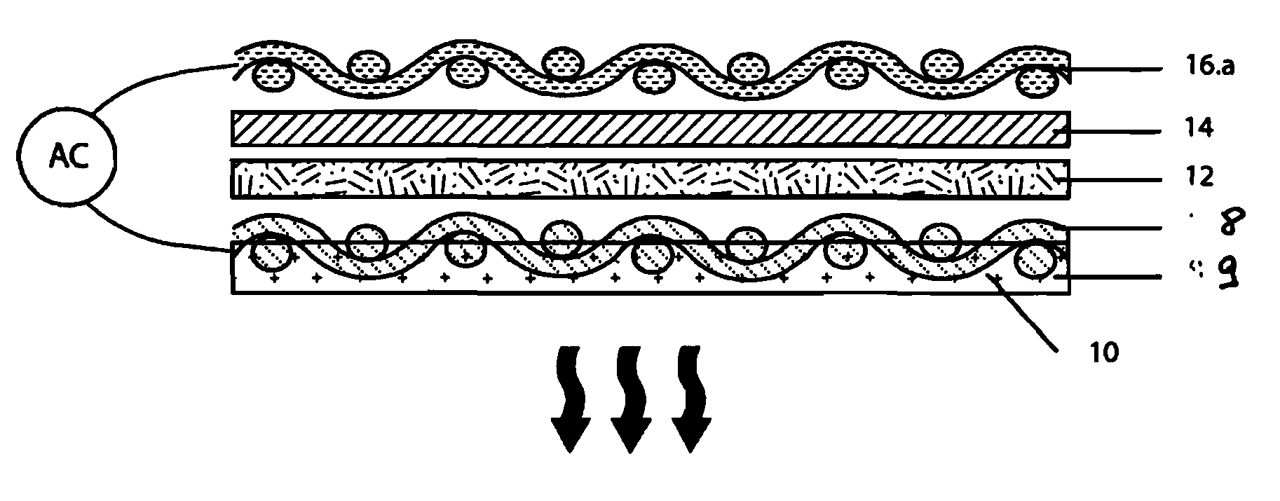
[0028]A PET fabric material 8 (in the example: PET 1000 120-23, manufacturer: Sefar, Thal, Switzerland) with silver-coated PET fibres (here: 120 fibres / cm, 23 μm thread diameter, thickness of the silver coating approx. 500 nm) is provided with a transparent polymer material 9 (here: an acrylic resin), so that a first planar and transparent electrode layer 10 is implemented. Contact can be made with this electrode layer 10 in the side region and it has a thickness of typically between 30 μm and 200 μm. In this manner a layer is formed, which on one planar side is non-conducting, and on its other planar side is conducting.

[0029]Onto this first electrode layer, which in the design shown enables a transmission factor for visible light of approx. 50%, an active layer 12 is provided by means of screen printing (or other suitable coating application methods). In a particularly preferred manner, this active layer is also applied by means of an endless process by means of suitable coating a...


PUM


Abstract

An optoelectronic film assembly, has a first flat electrode layer, a second flat electrode layer as a counter electrode to the first flat electrode layer, a dielectric layer between the electrode layers and an active layer provided next to the dielectric layer and arranged between the electrode layers and made of an electroluminescent material. To this end, the first and / or the second electrode layers are implemented to be translucent and TCO-free, particularly ITO-free, by using a woven fabric comprising electrically conductive fibers.

Description

BACKGROUND[0001]The present invention concerns an optoelectronic film arrangement, in particular an electroluminescence (EL) film, in accordance with the preamble of the main claim.[0002]Such devices are of general known art from the prior art, and by virtue of their advantageous planar lighting properties in conjunction with low power consumption and extended lighting times, are deployed in a very wide variety of application fields, primarily in the implementation of warning or message surfaces in lighting, advertising, design and architecture.[0003]Planar, film-type electroluminescence devices are based on the functional principle that a so-called active layer, typically consisting of doped zinc sulphide as an electroluminescent material, and a dielectric layer, are provided between two planar electrodes in the manner of a plate condenser, and that this arrangement, when powered by an alternating voltage signal (with a typical frequency between approx. 200 Hz and 4 kHz) emits a co...

Claims


Application Information

Patent Timeline
IPC IPC(8): H05B33/28H05B33/10
CPCH01L51/0097H01L51/442Y02E10/549H05B33/28H05B33/14Y02P70/50H10K77/111H10K30/82
Inventor CHABRECEK, PETERMEIER, HANSPETERLANTUS, MURIELSONDEREGGER, URIEL
Owner SEFAR THAL
Why Eureka
Try Eureka