
Semiconductor device having lateral diode

a technology of lateral diodes and semiconductor devices, which is applied in the direction of diodes, semiconductor devices, electrical devices, etc., can solve the problems of avalanche breakdown and inability to improve avalanche capability, and achieve the effect of improving avalanche capability and reverse recovery capability

Inactive Publication Date: 2012-02-09
DENSO CORP
View PDF5 Cites 17 Cited by
  • Summary
  • Abstract
  • Description
  • Claims
  • Application Information

AI Technical Summary

Benefits of technology

The present invention provides a semiconductor device with a lateral diode that has improved reverse recovery capability and avalanche capability. The semiconductor device includes a semiconductor substrate, a first semiconductor region, a first conductivity-type contact region, a first electrode, a second semiconductor region, a second electrode, and an isolation structure. The second semiconductor region includes a low impurity concentration portion, a high impurity concentration portion, and an extension portion. The second electrode forms an ohmic contact with the high impurity concentration portion. The semiconductor device also includes a second conductivity-type extension portion located in the semiconductor layer and having an impurity concentration greater than the impurity concentration of the low impurity concentration portion and the high impurity concentration portion. The technical effect of the present invention is to provide a semiconductor device with a lateral diode that has improved performance and reliability.

Problems solved by technology

However, the avalanche capability cannot be improved.
Therefore, it is likely that the avalanche breakdown occurs during a high speed switching operation.

Method used


Image

  • Semiconductor device having lateral diode
  • Semiconductor device having lateral diode
  • Semiconductor device having lateral diode

Examples


first embodiment

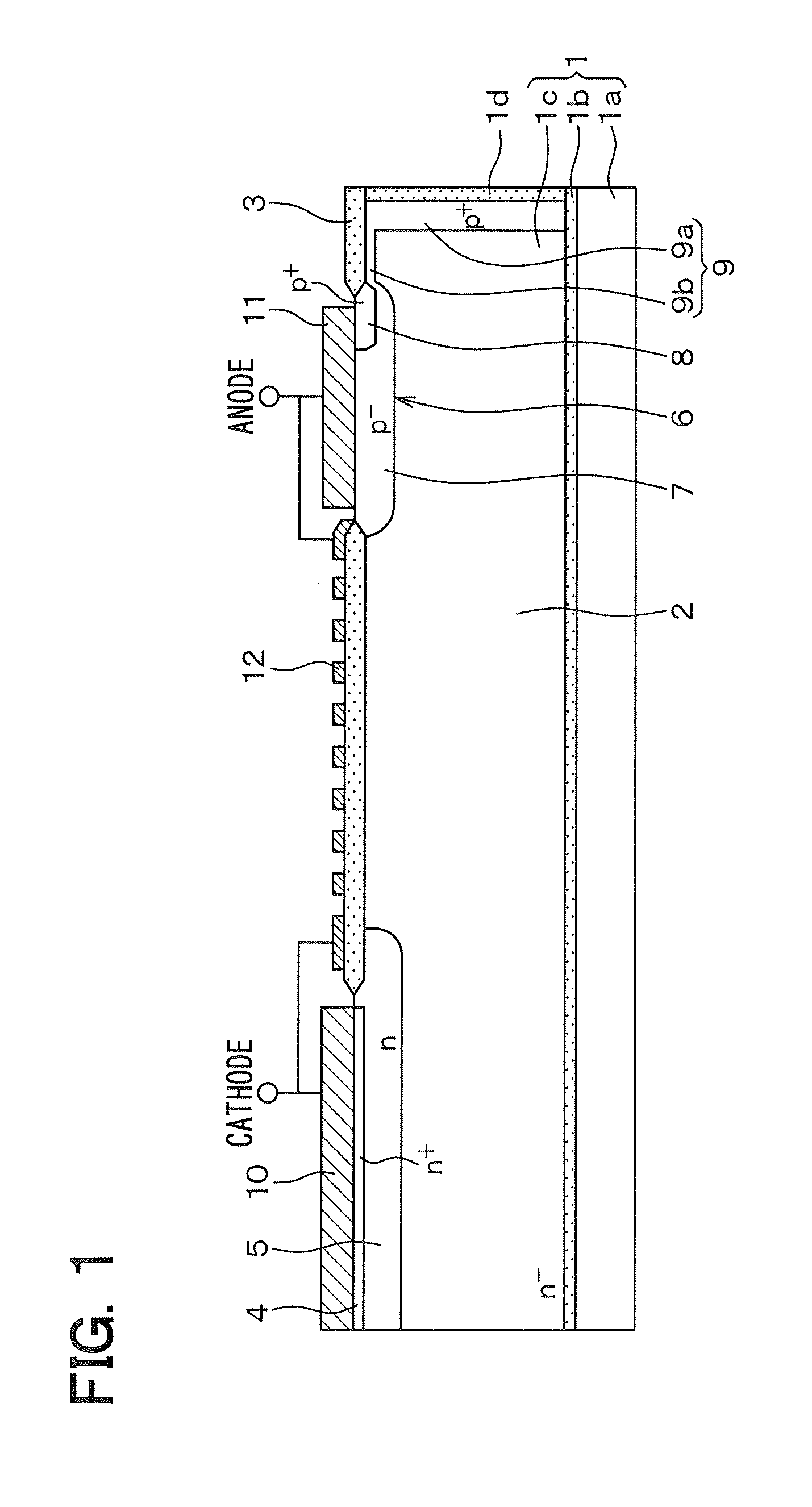
[0046]A semiconductor device having a lateral diode according to a first embodiment of the present invention is described below with reference to FIGS. 1, and 2A and 2B. FIG. 1 is a cross-sectional view of the semiconductor device taken along the line I-I in FIG. 2B. FIG. 2A is a top view of one cell of the lateral diode of the semiconductor device. FIG. 2B is an enlarged view taken within a region R in FIG. 2A.

[0047]According to the first embodiment, as shown in FIG. 1, the lateral diode is formed by using a semiconductor substrate 1 as a SOI substrate. The semiconductor substrate 1 includes a supporting substrate 1a, a buried oxide (BOX) layer 1b on the supporting substrate 1a, and an active layer 1c on the BOX layer 1b. For example, the supporting substrate 1a can be a silicon substrate, and the active layer 1c can be a silicon layer. According to the first embodiment, the active layer 1c serves as an n−-type cathode layer 2. Each part of the lateral diode is formed in the cathod...

second embodiment

[0080]A second embodiment of the present invention is described below with reference to FIG. 9. A difference between the first and second embodiments is the structure of the anode extension portion 9.

[0081]FIG. 9 is a diagram illustrating a cross-sectional view of a semiconductor device having a lateral diode according the second embodiment. As shown in FIG. 9, according to the second embodiment, the thickness of the first portion 9a of the anode extension portion 9 is less than the active layer 1c. Specifically, the first portion 9a extends from the surface of the active layer 1c and is terminated inside the active layer 1c without reaching the BOX layer 1b. Thus, about an upper half of the side surface of the trench isolation structure 1d is covered with the first portion 9a, but about a lower half of the side surface of the trench isolation structure 1d is not covered with the first portion 9a. About the lower half of the trench isolation structure 1d is in contact with the catho...

third embodiment

[0084]A third embodiment of the present invention is described below with reference to FIG. 10. A difference between the first and third embodiments is the structure of the anode extension portion 9.

[0085]FIG. 10 is a diagram illustrating a cross-sectional view of a semiconductor device having a lateral diode according the third embodiment. As shown in FIG. 10, according to the third embodiment, the thickness of the first portion 9a of the anode extension portion 9 is less than the active layer 1c. Specifically, like the second embodiment, the first portion 9a extends from the surface of the active layer 1c and is terminated inside the active layer 1c without reaching the BOX layer 1b.

[0086]Further, according to the third embodiment, the anode extension portion 9 has no second portion 9b. Therefore, the first portion 9a is separated from the anode region 6.

[0087]Even in such a structure as shown in FIG. 10, the depletion layer can extend from the anode extension portion 9 including...


PUM


Abstract

A semiconductor device having a lateral diode includes a semiconductor layer, a first semiconductor region in the semiconductor layer, a contact region having an impurity concentration greater than that of the first semiconductor region, a second semiconductor region located in the semiconductor layer and separated from the contact region, a first electrode electrically connected through the contact region to the first semiconductor region, and a second electrode electrically connected to the second semiconductor region. The second semiconductor region includes a low impurity concentration portion, a high impurity concentration portion, and an extension portion. The second electrode forms an ohmic contact with the high impurity concentration portion. The extension portion has an impurity concentration greater than that of the low impurity concentration portion and extends in a thickness direction of the semiconductor layer.

Description

CROSS REFERENCE TO RELATED APPLICATION[0001]This application is based on and claims priority to Japanese Patent Application No. 2010-175464 filed on Aug. 4, 2010 and No. 2011-118863 filed on May 27, 2011, the contents of which are incorporated herein by reference.FIELD OF THE INVENTION[0002]The present invention relates to a semiconductor device having a lateral diode.BACKGROUND OF THE INVENTION[0003]U.S. Pat. No. 5,982,015 corresponding to JP-A-11-233795 discloses a lateral diode used as a freewheeling diode (FWD) connected in parallel to a semiconductor switching element such as an insulated gate bipolar transistor (IGBT). The anode of the lateral diode has both ohmic contact and Schottky contact so that the accumulation of holes can be reduced. Accordingly, the reverse recovery charge Qrr is reduced so that the reverse recovery capability can be improved. That is, the Schottky contact reduces the electronic injection. Therefore, even when the hole injection can be reduced without...

Claims


Application Information

Patent Timeline
Patent Type & Authority Applications(United States)
IPC IPC(8): H01L29/861
CPCH01L27/0664H01L29/0615H01L29/0692H01L29/0878H01L29/868H01L29/405H01L29/42368H01L29/7394H01L29/7824H01L29/1095
Inventor YAMAMOTO, TAKAOTOKURA, NORIHITOKATO, HISATONAKAGAWA, AKIO
Owner DENSO CORP
Learn More