
Ldpmos structure for enhancing breakdown voltage and specific on resistance in bicmos-DMOS process

a technology of bicmos and dmos, applied in the field of ldpmos structure for enhancing breakdown voltage and specific on resistance in bicmos-dmos process, can solve the problems that approaches tending to maximize bvd tend to also adversely affect rsub>onsp /sub>and vice versa

Active Publication Date: 2011-12-15
MACRONIX INT CO LTD
View PDF2 Cites 36 Cited by
  • Summary
  • Abstract
  • Description
  • Claims
  • Application Information

AI Technical Summary

Benefits of technology

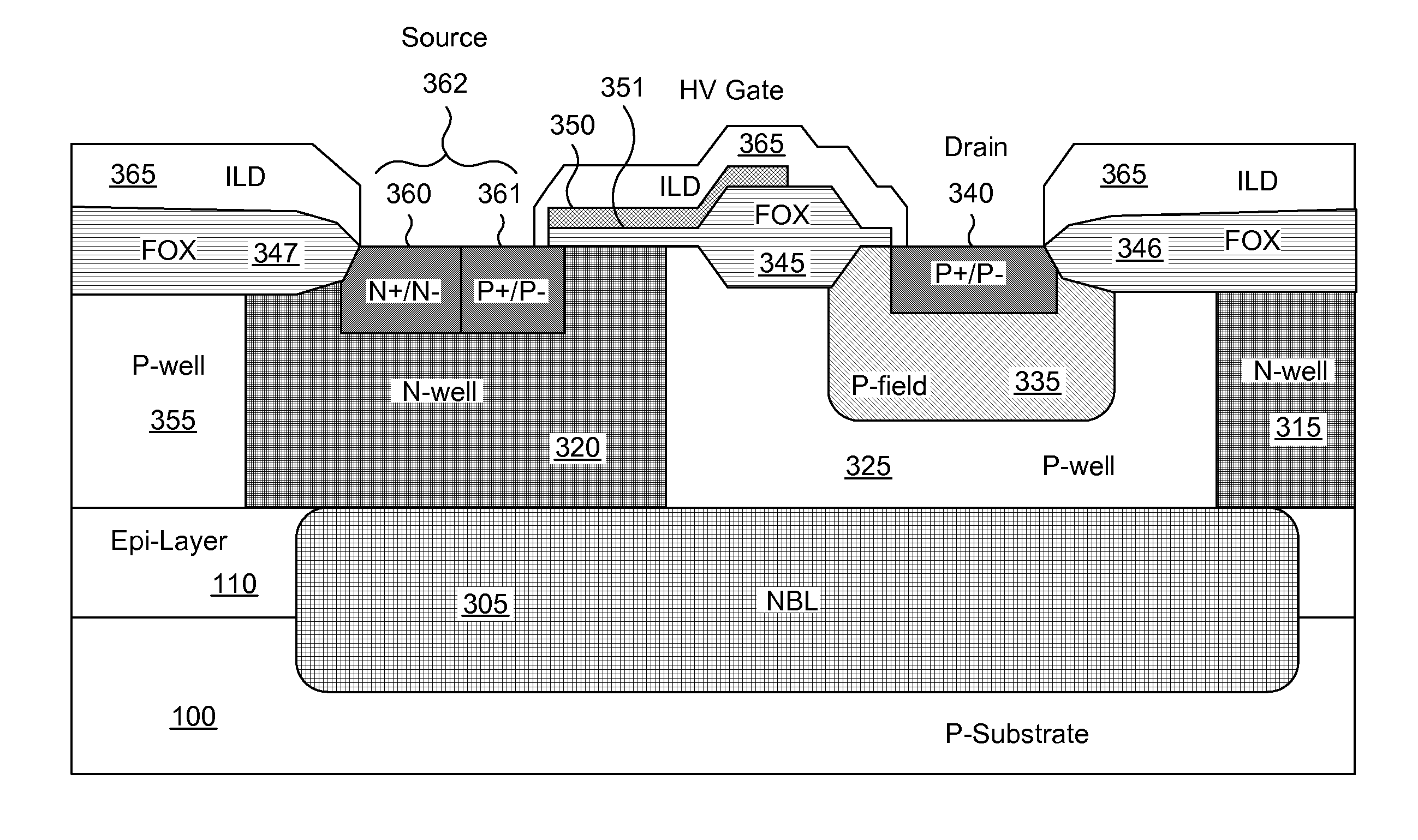
[0006]The present invention addresses this need by providing a semiconductor structure that exhibits an efficient trade-off between breakdown voltage (BVD) and specific on-resistance (Ronsp). The invention herein disclosed comprises, according to one embodiment, a substrate formed of a first conductivity type with an epitaxial layer formed over the substrate. A first well region of a second conductivity type may be formed in the epitaxial layer with a second well region of the second conductivity type likewise formed in the epitaxial layer and spaced apart from the first well region. A third well region of the first conductivity type may be formed between the first well region and the second well region. A field region of the first conductivity type may be formed in a surface of the third well region and spaced apart from the first and second well regions, the field region having a drain region of the first conductivity type formed on a surface thereof and extending into the field region.

Problems solved by technology

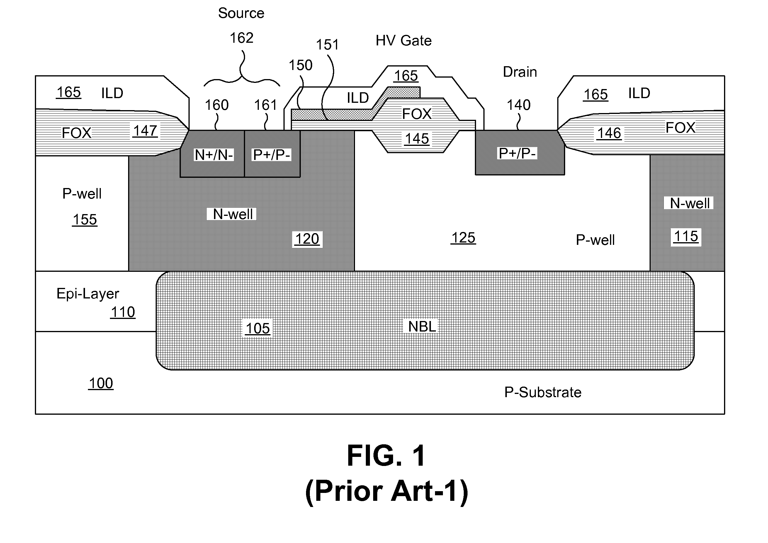
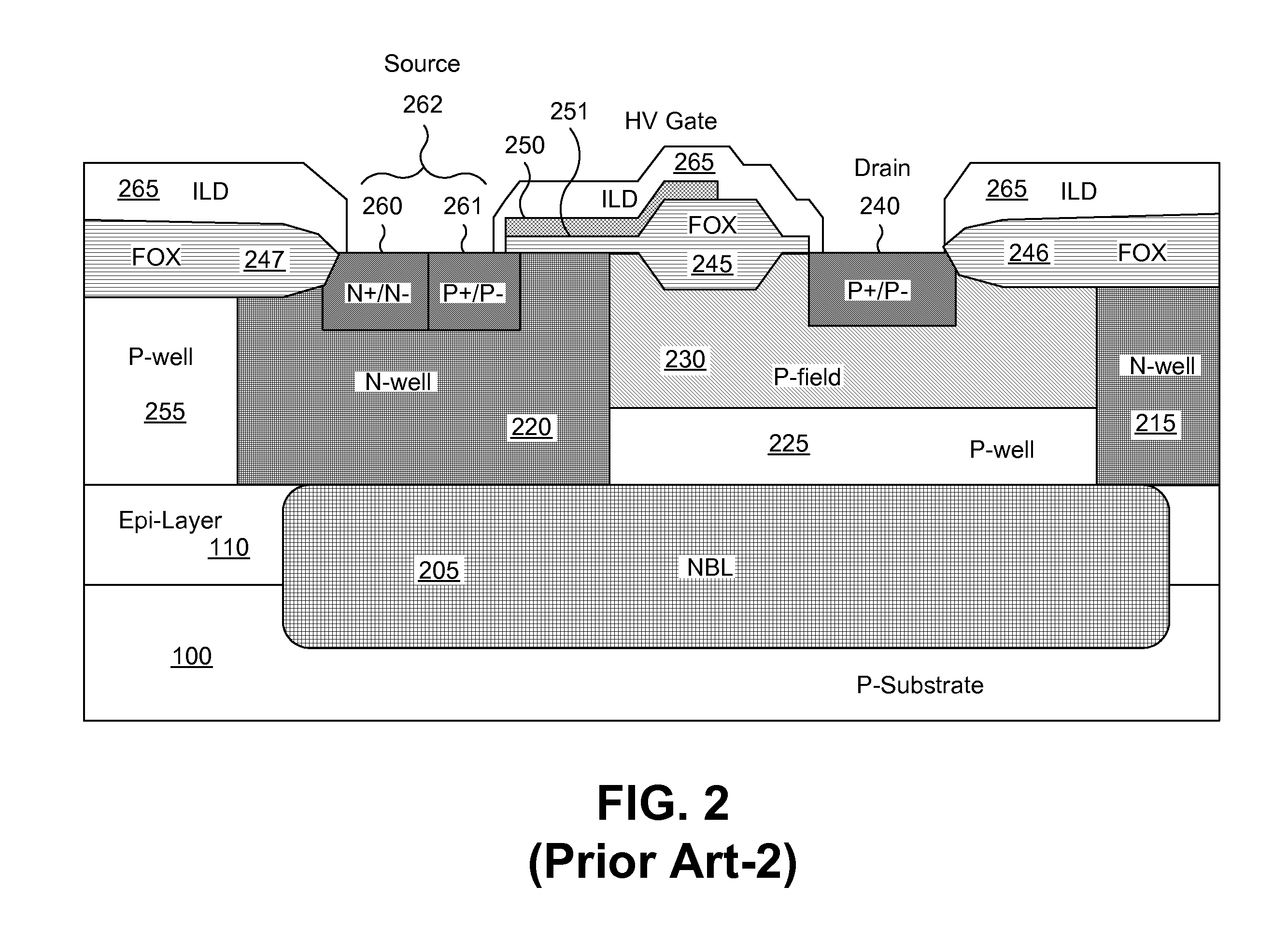
One problem encountered when designing such LDPMOS devices is that approaches tending to maximize BVD tend also adversely to affect the Ronsp and vice versa.

Method used


Image

  • Ldpmos structure for enhancing breakdown voltage and specific on resistance in bicmos-DMOS process
  • Ldpmos structure for enhancing breakdown voltage and specific on resistance in bicmos-DMOS process
  • Ldpmos structure for enhancing breakdown voltage and specific on resistance in bicmos-DMOS process

Examples


Embodiment Construction

[0023]Embodiments of the invention are now described and illustrated in the accompanying drawings, instances of which are to be interpreted to be to scale in some implementations while in other implementations, for each instance, not. In certain aspects, use of like or the same reference designators in the drawings and description refers to the same, similar or analogous components and / or elements, while according to other implementations the same use should not. According to certain implementations, use of directional terms, such as, top, bottom, left, right, up, down, over, above, below, beneath, rear, and front, are to be construed literally, while in other implementations the same use should not. The present invention may be practiced in conjunction with various integrated circuit fabrication and other techniques that are conventionally used in the art, and only so much of the commonly practiced process steps are included herein as are necessary to provide an understanding of th...


PUM


Abstract

An LDPMOS structure having enhanced breakdown voltage and specific on-resistance is described, as is a method for fabricating the structure. A P-field implanted layer formed in a drift region of the structure and surrounding a lightly doped drain region effectively increases breakdown voltage while maintaining a relatively low specific on-resistance.

Description

BACKGROUND OF THE INVENTION[0001]1. Field of the Invention[0002]The present invention relates generally to semiconductors and, more particularly, to power metal-oxide-semiconductor transistors and methods of fabricating and using same.[0003]2. Description of Related Art[0004]A lateral double-diffused metal-oxide-semiconductor (LDMOS) field effect transistor (MOSFET) is a MOSFET fabricated with coplanar drain and source regions. LDMOS devices with a P-channel may be referred to as LDPMOS devices. These devices are typically used in high voltage applications. When designing such LDPMOS devices, it is important for the device to have a very high breakdown voltage (BVD) whilst also exhibiting, during operation, a low specific on-resistance (Ronsp). By designing LDPMOS devices with low Ronsp and high BVD, low power loss can be achieved in high voltage applications. In addition, a low Ronsp can facilitate a high drain current (Idsat) when the transistor is in saturation. One problem encou...

Claims


Application Information

Patent Timeline
Patent Type & Authority Applications(United States)
IPC IPC(8): H01L29/78H01L21/336
CPCH01L21/8249H01L27/0623H01L29/0847H01L29/7835H01L29/42368H01L29/66659H01L29/1083
Inventor HUANG, YIN-FUCHUNG, MIAO-CHUNLIEN, SHIH-CHIN
Owner MACRONIX INT CO LTD
Learn More