
Electron microscope specimen and method for preparing the same

Inactive Publication Date: 2011-12-01
MICRON TECH INC
View PDF5 Cites 5 Cited by
  • Summary
  • Abstract
  • Description
  • Claims
  • Application Information

AI Technical Summary

Benefits of technology

[0012]By using a dicing process and a thinning process in the present invention, a specimen with superior structure can be obtained. The problem of missing wedge resulted from the obstruction of the sample base in conventional arts can be prevented.

Problems solved by technology

However, as the integration of semiconductor devices are upgrading and various semiconductor devices with special structure are proposed, current two-dimensional image analysis techniques are unable to reflect the device structure precisely, especially those devices with high curvature structure, for example, via structures.
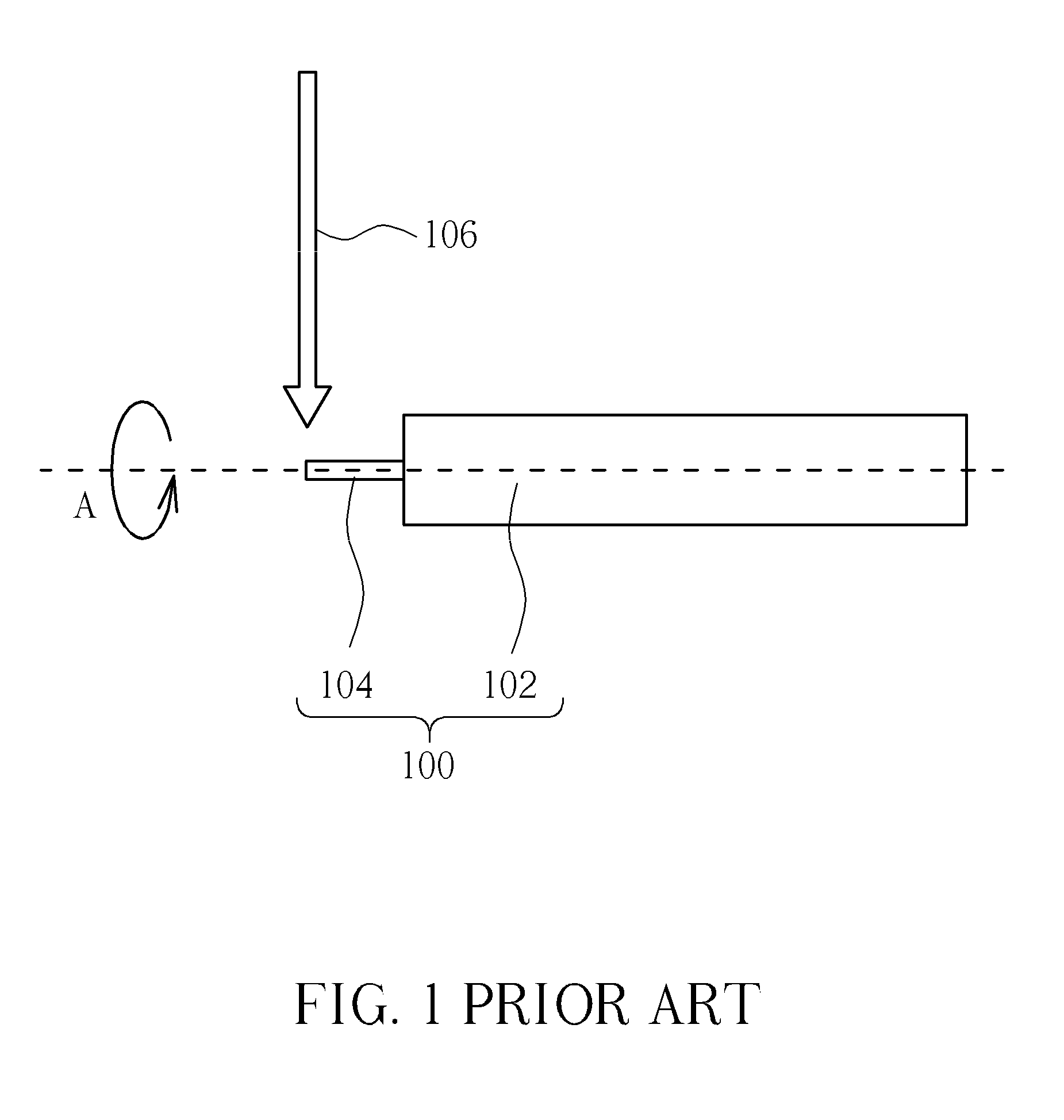
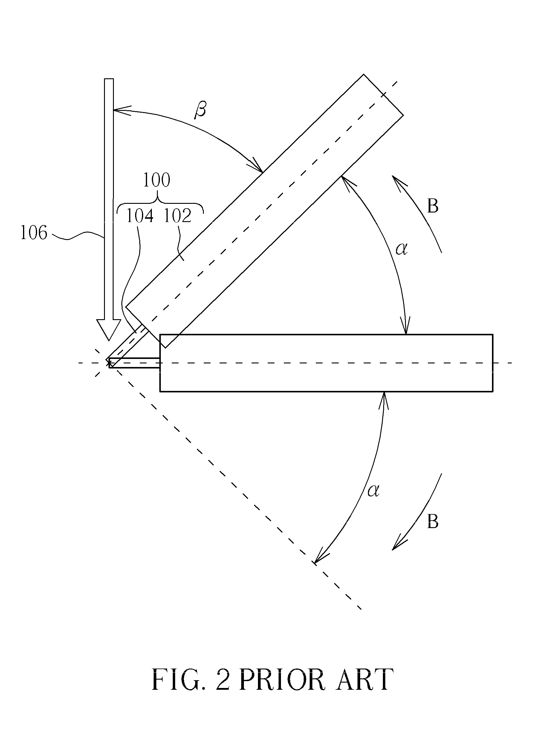
However, the conventional design of the base portion 102 and the sample 104 has an inherent limitation, which is also known as missing-wedge phenomenon.

Method used


Image

  • Electron microscope specimen and method for preparing the same
  • Electron microscope specimen and method for preparing the same
  • Electron microscope specimen and method for preparing the same

Examples


Embodiment Construction

[0017]The present invention now will be described more fully hereinafter with reference to the accompanying drawings, in which preferred embodiments of the invention are shown. This invention may, however, be embodied in many different forms and should not be construed as limited to the embodiments set forth herein; rather, these embodiments are provided so that this disclosure will be thorough and complete, and will fully convey the scope of the invention to those skilled in the art.

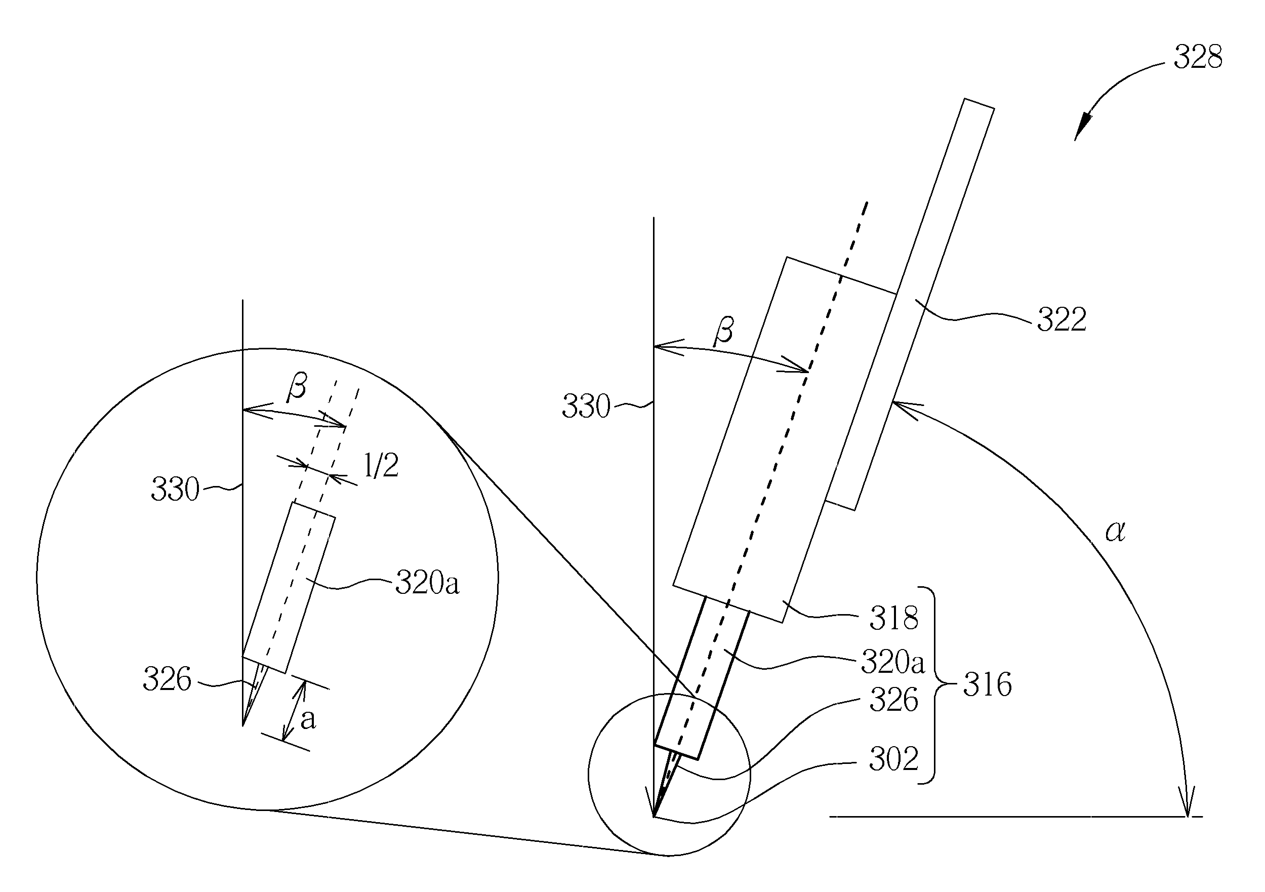
[0018]FIG. 3 to FIG. 10 are schematic diagrams showing the method for preparing the electron microscope specimen according to one embodiment of the present invention. As shown in FIG. 3, a wafer sample 300 is provided. An analysis region (or an analysis spot) 302 is defined on the surface of the wafer sample 300. Microstructures to be analyzed are located in the analysis region 302. The wafer sample 300 is preferably a semiconductor wafer piece. However, the wafer sample 300 may be any material that can...


PUM


Abstract

A method for preparing an electron microscope specimen is provided. The method includes providing a wafer sample with an analysis region disposed thereon. A dicing process is performed to cut a sample piece from the wafer sample. The sample piece includes a target pillar structure wherein the analysis region is located on a top portion of the target pillar structure. A thinning process is performed to thin the top portion of the target pillar structure. The invention further provides an electron microscope specimen and a method of forming a 3D image.

Description

BACKGROUND OF THE INVENTION[0001]1. Field of the Invention[0002]The present invention relates to an electron microscope specimen and the preparing method thereof, and more particularly, to an electron microscope specimen which is suitable for constructing a three-dimensional image and the preparing method thereof.[0003]2. Description of the Prior Art[0004]With the miniaturization of semiconductor devices, the analysis techniques for observing the microstructure of semiconductor devices have become increasingly important. For example, the microstructure of the semiconductor devices can be observed by using a scanning electron microscopy (SEM) or a transmission electron microscopy (TEM). Due to the better resolution, TEM is widely used in analyzing semiconductor devices.[0005]However, as the integration of semiconductor devices are upgrading and various semiconductor devices with special structure are proposed, current two-dimensional image analysis techniques are unable to reflect th...

Claims


Application Information

Patent Timeline
IPC IPC(8): G01N23/00
CPCG01N1/286G01N2001/2873G01N23/2251
Inventor LUO, JIAN-SHINGHSU, WEN-SHAN
Owner MICRON TECH INC
Learn More