Substrate with transparent conductive film and thin film photoelectric conversion device

Active Publication Date: 2011-12-01
KANEKA CORP
View PDF2 Cites 34 Cited by
  • Summary
  • Abstract
  • Description
  • Claims
  • Application Information

AI Technical Summary

Benefits of technology

[0030]According to the invention, a substrate with transparent conductive film is obtained in which an underlying layer 2 having a irregular structure and a transparent conductive film 4 are stacked in this order on a transparent insulating substrate, and the top-bottom distance (H1) of the irregular structure of the underlying layer is larger than the top-bottom distance (H2) of the irregular structure of the transparent conductive film.
[0031]For example, nano-imprinting method is used in which a mold 3 of a silicon wafer etched with an acid or alkali is transcribed onto the underlying layer over the transparent insulating substrate to form an irregular structure in the underlying layer 2. By the nano-imprinting method, a texture with large irregularities is formed therein. Since this large irregularity-size texture has a pyramidal or inverse-pyramidal irregularity structure, light scattering of incident light having long wavelengths is increased on the interface between the underlying layer 2 and the transparent conductive film 4 while reflection on the interface is decreased. The transparent conductive film 4 is composed of at least two transparent electrode layers, and the outermost layer of the layers, i.e., a second transparent electrode layer 4b is deposited by low-pressure CVD; therefore, a texture with small irregularities is formed in the surface of the transparent conductive film. Due to this small irregularity-size texture, light rays having a shorter wavelength range are scattered on the interface between the transparent conductive film 4 and the photoelectric conversion unit.
[0032]For this reason, a thin film photoelectric conversion device using the substrate with transparent conductive film of the invention produces a highly advantageous effect of confining incident light over wide wavelength range, so that a photoelectric current is increased therein. The invention contributes largely to, in particular, a multi-junction type photoelectric conversion device in which two or more photoelectric conversion units having absorbable wavelength ranges different from each other are stacked. Additionally, in the substrate with a transparent conductive film of the invention, the size of the irregularities in the outermost surface of the transparent conductive film is small. Thus, in a semiconductor layer deposited on the transparent conductive film, defects are prevented from being generated from the recesses, as nucleation points, so that the open circuit voltage (Voc) of the device is not easily reduced. By the combined effect of the restraint on the reduction in the open circuit voltage with the photoelectric-current-increase, the conversion efficiency of the photoelectric conversion device is improved.
[0033]In the invention, zinc oxide is deposited as the second transparent electrode layer 4b, which is the outermost layer of the transparent conductive film 4, by low-pressure CVD, whereby a texture with a small irregularity size is formed in the surface of the transparent conductive film 4. In this way, the texture with small irregularity size can easily be produced, and therefore a substrate with transparent conductive film which has a light scattering effect in a wide wavelength range can be produced at low costs.

Problems solved by technology

However, the method has drawbacks that a surface having fine irregularities is not easily obtained, and the area of the surface is not easily made large, either.
However, high temperature is required for softening the glass in order to form the irregular structure in the glass.
Moreover, the size of the recesses and projections is limited so that satisfactory effects are not necessarily obtained for light scattering of wavelengths in a wide range.
However, in the same manner as described above, the size of the each irregular structure is limited.
Moreover, because of the use of the sol-form electrode, a high-quality film is not easily formed.
Thus, the step of producing the transparent conductive film is complicated.
Further the texture formed of the first oxide material is discontinuous, and therefore, the surface of the transparent conductive film has many flat areas.
Thus, in a semiconductor layer, such as a silicon layer, which is deposited on the transparent conductive film, defects are easily generated from the recesses as nucleation points.
Thus, there remains a problem that, in particular, the open circuit voltage (Voc) is reduced.

Method used


Image

  • Substrate with transparent conductive film and thin film photoelectric conversion device
  • Substrate with transparent conductive film and thin film photoelectric conversion device
  • Substrate with transparent conductive film and thin film photoelectric conversion device

Examples


example 1

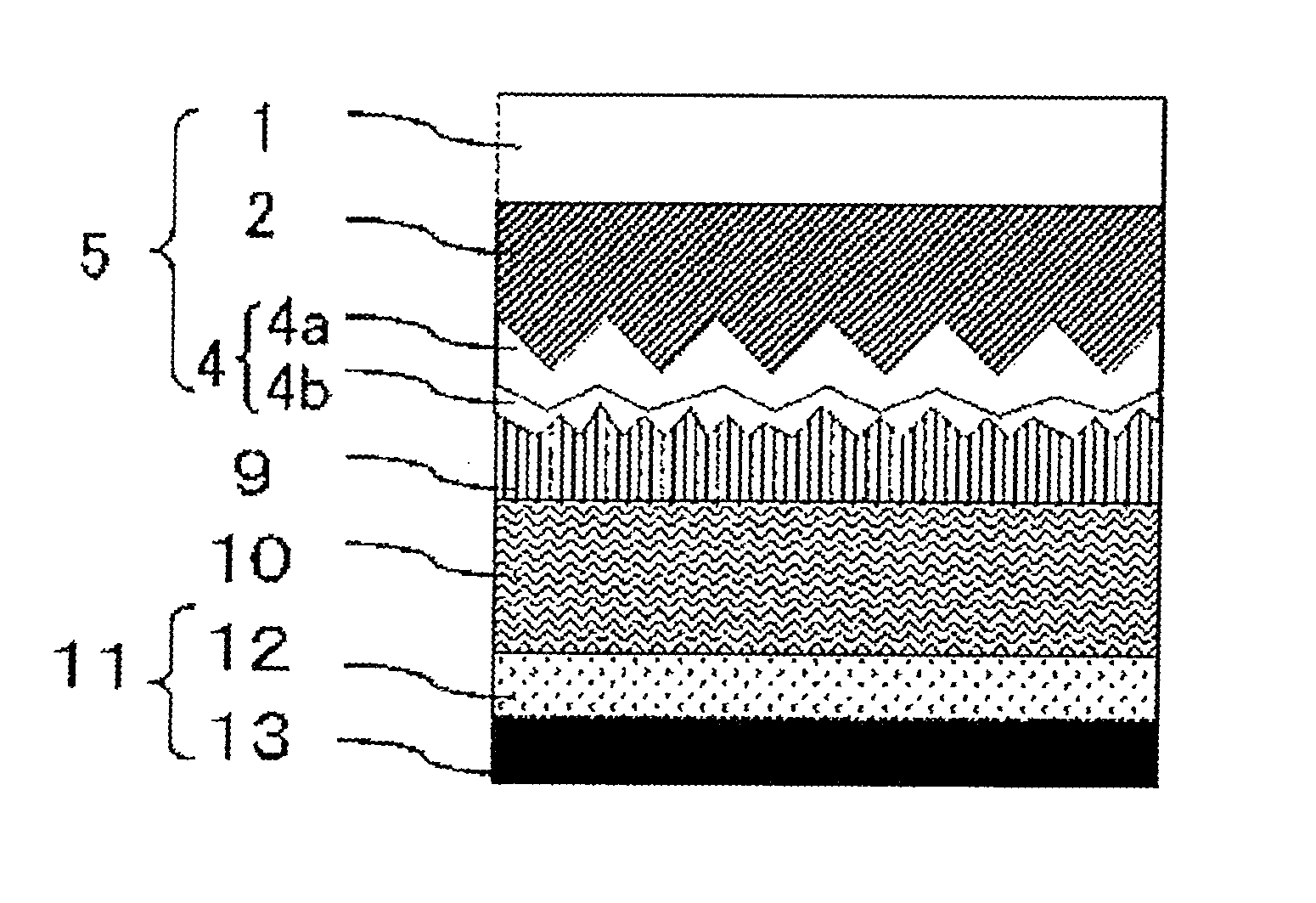
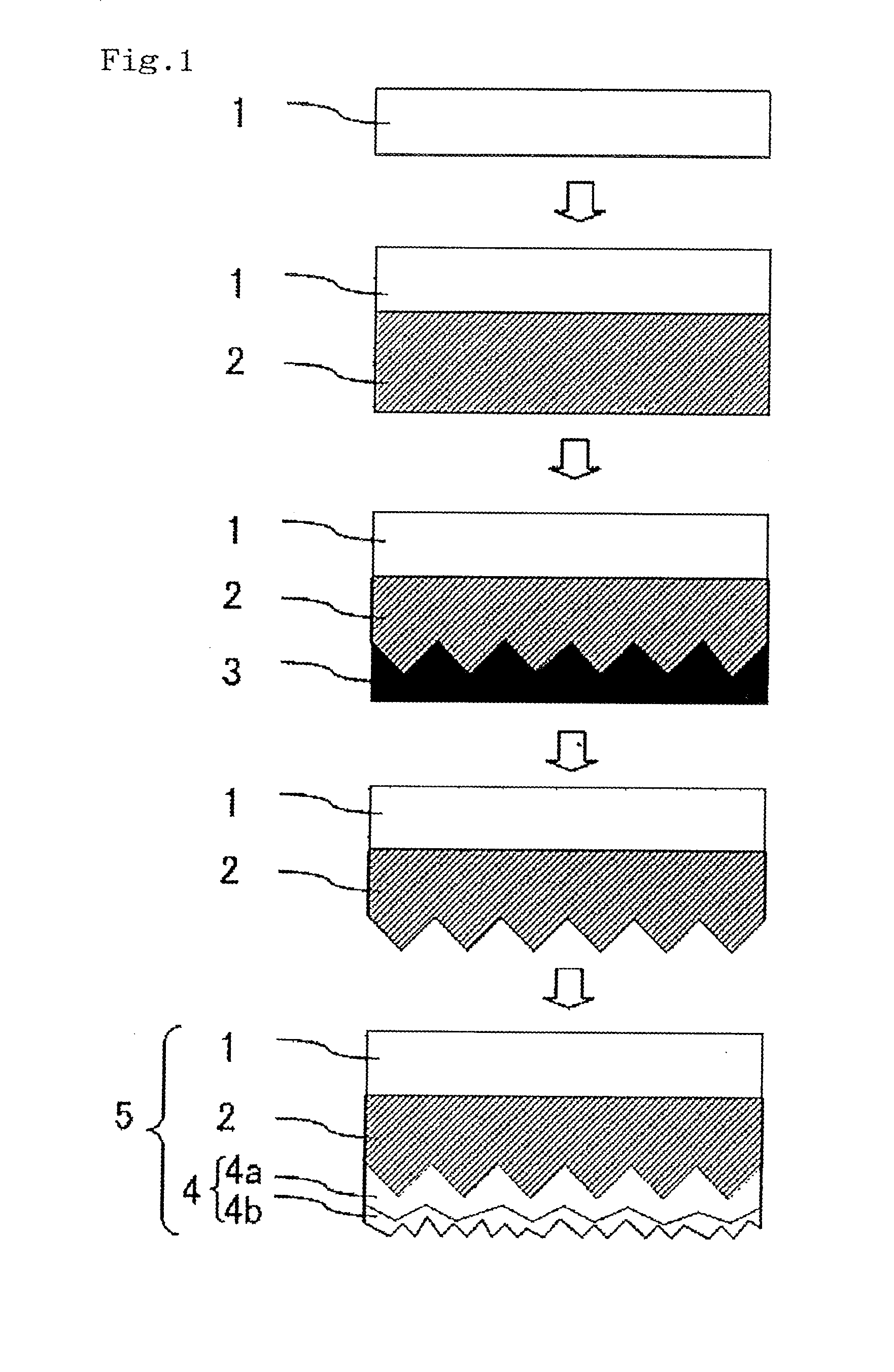
[0125]A double-junction type thin film photoelectric conversion device as illustrated in FIG. 3 was produced as Example 1.

[0126]First, an SiO2 layer was deposited, as an underlying layer 2, onto a glass substrate 1 having 0.7 mm thick and 125 mm square, by a sol-gel process. A coating solution used therefor was a SiO2 sol-gel solution (trade name: 512B, manufactured by Honeywell International, Inc.), which is used as an SOG material. A coating method used therefor was spin coating and the layer was formed into a film thickness of 1000 nm.

[0127]Next, the whole of the substrate on which the underlying layer 2 was formed was pre-baked on a hot plate at 60° C. for 20 minutes to semi-cure the underlying layer. Subsequently, the substrate was transported into an imprinting device to push, against the underlying-layer-2-formed substrate, a mold 3 in which an irregular structure of was formed in a surface of a monocrystalline silicon substrate. The irregularities were in the shape of pyrami...

example 2

[0138]A double-junction type thin film silicon solar cell was formed as Example 2 in the same way as in Example 1. However, in Example 2, the method for depositing a first transparent electrode layer 4a was different from that in Example 1.

[0139]First, an underlying layer 2 was formed onto a glass substrate 1 by a sol-gel method to form an inverse-pyramidal-irregular structure into the surface of the underlying layer by the same nano-imprinting method as in Example 1. The first transparent electrode layer 4a was deposited into a thickness of 1200 nm on the substrate on which the underlying layer was deposited by low-pressure CVD. At the time of the completion of the deposition, the supply of diethyl zinc, water, diborane, and phosphine as raw material gases was stopped, thereby interrupting deposition once. Thereafter, the raw material gases were again supplied to deposit a second transparent electrode layer 4b into a thickness of 400 nm.

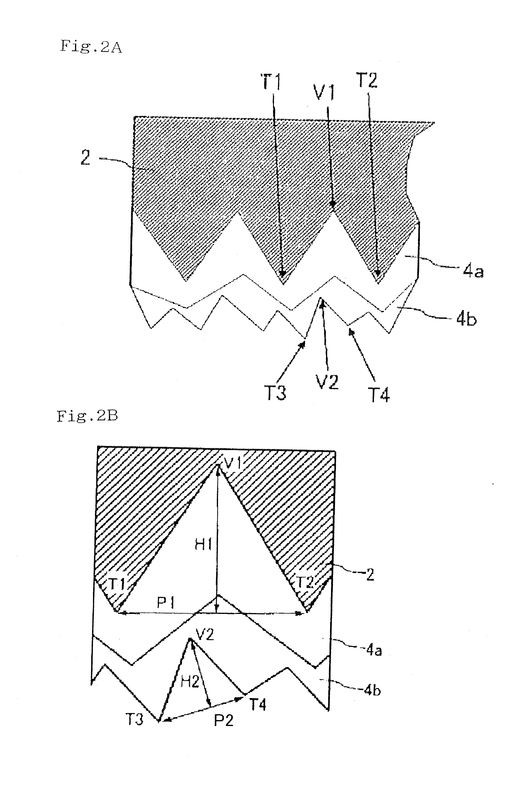
[0140]AFM was used to observe the surface sha...

example 3

[0157]A double-junction type thin film photoelectric conversion device as illustrated in FIG. 3 was formed as Example 3. Example 3 was different from Example 1 only in that the first transparent electrode layer 4a was changed from zinc oxide to indium-titanium composite oxide.

[0158]In the same way as in Example 1, an underlying layer and an irregular structure were formed, and then indium oxide doped with Ti was deposited, as a first transparent electrode layer 4a, into a thickness of 300 nm onto the underlying layer by sputtering. Thereafter, a transparent electrode layer 4b was deposited into a thickness of 400 nm thereon by low-pressure CVD. In this way, a transparent conductive film 4 was deposited. The deposition of the transparent electrode layer 4b was performed by CVD under the same conditions as in Example 1.

[0159]AFM was used to observe the surface shape of the transparent conductive film. The top-bottom distance H2 of the irregular structure was 90 nm, and the distance P2...


PUM


Abstract

Disclosed is a substrate with a transparent conductive film, wherein an underlying layer and a transparent conductive film are arranged in this order on a transparent insulating substrate. The transparent conductive film-side surface of the underlying layer is provided with a pyramid-shaped or inverse pyramid-shaped irregular structures, and the transparent conductive film comprises a first transparent electrode layer which is formed on the underlying layer and a second transparent electrode layer which forms the outermost surface of the transparent conductive film. By forming a zinc oxide layer that serves as the second transparent electrode layer by a reduced pressure CVD method, a substrate with a transparent conductive film that is provided with an irregular structure smaller than that of the underlying layer can be obtained. The substrate with a transparent conductive film can improve the conversion efficiency of a photoelectric conversion device through an increased light trapping effect.

Description

TECHNICAL FIELD[0001]The invention provides a means capable of improving the conversion efficiency of a thin film photoelectric conversion device, and relates in particular to an improvement in a transparent conductive film for a thin film photoelectric conversion device.BACKGROUND ART[0002]In recent years, attention has been paid to thin film photoelectric conversion devices, which have little problem about resources, and developments thereof have been actively made in order to reduce the costs of photoelectric conversion devices compatible with high efficiency thereof. A thin film silicon solar cell, which is one of the thin film photoelectric conversion devices, can be formed on a large-area glass substrate or stainless steel substrate at low temperature; thus, it can be expected that costs thereof are reduced. In order to improve the conversion efficiency of the thin film silicon solar cell, attempts for increasing the optical path of light incident into its photoelectric conver...

Claims


Application Information

Patent Timeline
IPC IPC(8): H01L31/0224H01J1/62H01L21/283H01L23/482
CPCH01L31/022466H01L31/02366H01L31/03921H01L31/0745H01L31/076Y02E10/548H01L31/1884H01L51/5203H01L51/5268H05B33/28H01L31/077H01L31/022483Y02E10/547H10K50/805H10K50/854
Inventor MEGURO, TOMOMIYAMAMOTO, KENJI
Owner KANEKA CORP
Why Eureka
Try Eureka