
MEMS device manufacturing method

Inactive Publication Date: 2011-09-22
DISCO CORP
View PDF5 Cites 0 Cited by
  • Summary
  • Abstract
  • Description
  • Claims
  • Application Information

AI Technical Summary

Benefits of technology

[0007]It is therefore an object of the present invention to provide a MEMS device manufacturing method which can manufacture MEMS devices without reducing the quality thereof.
[0010]According to the present invention, the break start point forming step is performed to form the break start point in the substrate along the areas corresponding to the crossing streets before forming the MEMS devices on the substrate. Accordingly, it is possible to eliminate the problem that the quality of the MEMS devices may be reduced due to the debris scattered or the influence of heat by the application of a laser beam. In the break start point forming step, the break start point is formed in the areas corresponding to the crossing streets set on the substrate before performing the device forming step and the substrate breaking step. Accordingly, in the substrate breaking step, the substrate having the MEMS devices on the front side can be easily divided into the individual MEMS devices by applying an external force to the substrate.

Problems solved by technology

Hei 10-305420, there is a problem such that debris scattered by the application of the laser beam may be deposited to the surface of each MEMS device and that the quality of each MEMS device may be reduced due to the influence of heat by the laser beam applied to the substrate.

Method used


Image

  • MEMS device manufacturing method
  • MEMS device manufacturing method
  • MEMS device manufacturing method

Examples


Embodiment Construction

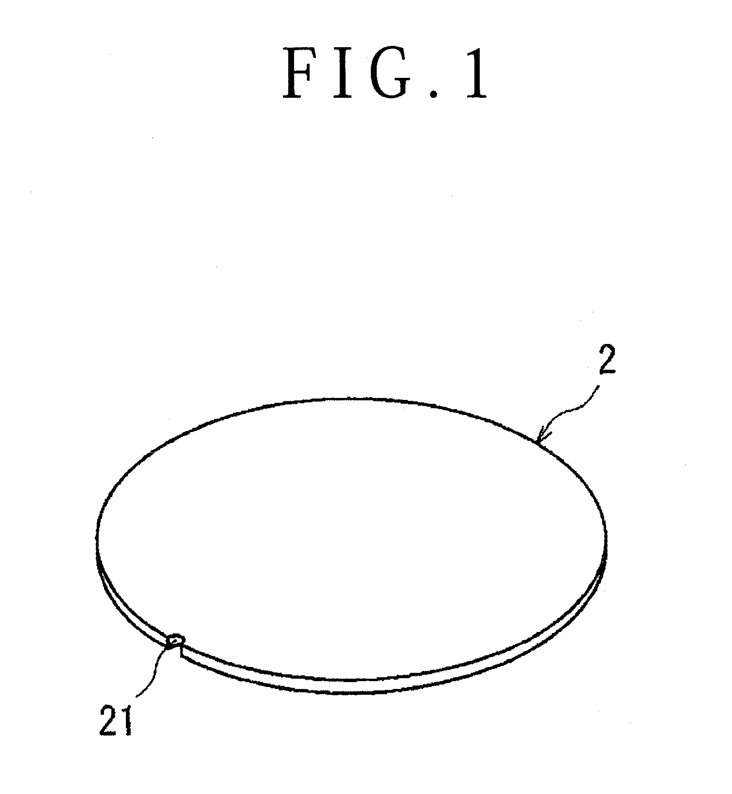
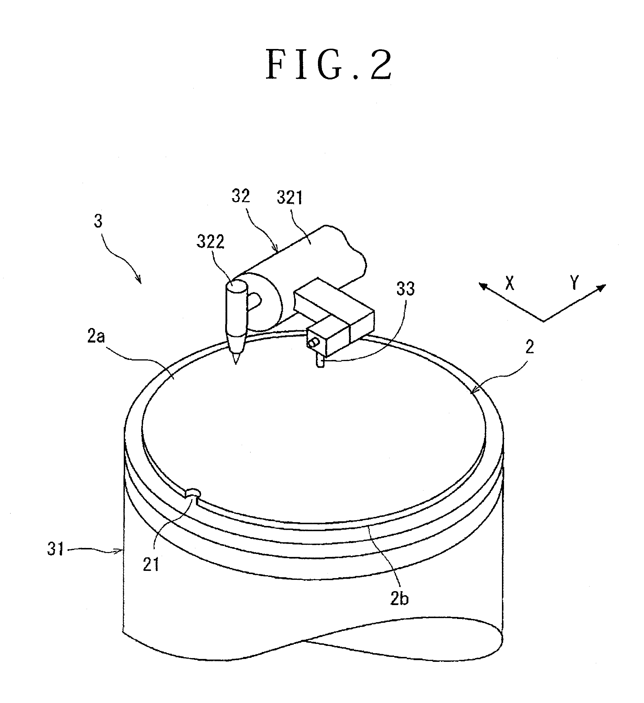
[0023]A preferred embodiment of the MEMS device manufacturing method according to the present invention will now be described in detail with reference to the attached drawings. FIG. 1 is a perspective view of a substrate 2 in the condition where a plurality of MEMS devices have not yet been formed thereon. The substrate 2 shown in FIG. 1 is formed from a glass substrate having a thickness of 200 μm, for example. The outer circumference of the substrate 2 is formed with a notch 21 for indicating a reference position. In manufacturing a plurality of MEMS devices by using the substrate 2 formed from a glass substrate shown in FIG. 1, a break start point forming step is first performed to form a break start point in the substrate 2 along the areas corresponding to a plurality of crossing streets set on the substrate 2 before forming a plurality of MEMS devices on the substrate 2.

[0024]This break start point forming step is performed by using a laser processing apparatus 3 shown in FIG. ...


PUM

PropertyMeasurementUnit
Poweraaaaaaaaaa
Poweraaaaaaaaaa
Frequencyaaaaaaaaaa

Abstract

A MEMS device manufacturing method including a break start point forming step of forming a break start point in a substrate along the areas corresponding to a plurality of crossing streets set on the substrate before forming a plurality of MEMS devices on the substrate, a device forming step of forming the MEMS devices in a plurality of areas partitioned by the areas corresponding to the crossing streets on the front side of the substrate after performing the break start point forming step, and a substrate breaking step of applying an external force to the substrate after performing the device forming step to thereby break the substrate along the areas corresponding to the crossing streets where the break start point is formed, thus dividing the substrate into the individual MEMS devices.

Description

BACKGROUND OF THE INVENTION[0001]1. Field of the Invention[0002]The present invention relates to a manufacturing method for Micro-Electro-Mechanical Systems (MEMS) devices such as acceleration sensors and pressure sensors.[0003]2. Description of the Related Art[0004]In a Micro-Electro-Mechanical Systems (MEMS) device fabrication process, a plurality of crossing division lines called streets are formed on the front side of a substantially disk-shaped substrate such as a glass substrate, silicon substrate, and organic substrate to thereby partition a plurality of areas where MEMS devices such as acceleration sensors, pressure sensors, gyroscopes, and tactile sensors are respectively formed. These areas where the MEMS devices are formed are divided from each other along the streets to thereby obtain the individual MEMS devices. As a dividing apparatus for dividing the substrate having the MEMS devices along the streets, a cutting apparatus called a dicing saw is generally used. This cu...

Claims


Application Information

Patent Timeline
IPC IPC(8): H01L21/02B23K26/00B23K26/40B28D5/00B81C99/00C03B33/09H01L21/301
CPCB23K26/063B23K26/0853B23K26/36B23K26/367H01L21/67132B23K2201/40B28D5/0011B81C1/00888H01L21/67092B23K26/4075B23K26/40B23K26/0622B23K26/364B23K2101/40B23K2103/50
Inventor ABATAKE, JUN
Owner DISCO CORP
Learn More