Method for forming ohmic electrode and semiconductor light emitting element

a technology of ohmic electrodes and light emitting elements, which is applied in the direction of basic electric elements, semiconductor devices, electrical equipment, etc., can solve the problems of low thermal stability, difficult to implement high power, and inability to achieve high power, etc., to achieve excellent light reflectivity, suppress external diffusion of reflective layers, and enhance light availability

Active Publication Date: 2011-09-01
SEOUL VIOSYS CO LTD
View PDF5 Cites 3 Cited by
  • Summary
  • Abstract
  • Description
  • Claims
  • Application Information

AI Technical Summary

Benefits of technology

[0012]The present invention is to provide a method for forming an ohmic electrode, wherein a reflective layer is formed of Ag or Al with excellent light reflectivity, a bonding layer is positioned under the reflective layer to reduce contact resistance, and a protective layer is positioned over the reflective layer so that a deterioration phenomenon is prevented, thereby simultaneously satisfying low contact resistance, high light reflectivity and high thermal stability; and a semiconductor light emitting element using the ohmic electrode.
[0027]As described above, according to the present invention, an ohmic electrode is formed by laminating a bonding layer, a reflective layer and a protective layer, heat treating them to form oxide films on the bonding layer and the protective layer, and suppressing the external diffusion of the reflective layer through the oxide films. Accordingly, the following effects can be expected.
[0028]First of all, since a reflective layer is formed of Ag, Al or an alloy including at least one of the foregoing with excellent light reflectivity, the light availability is enhanced. Further, since contact resistance between a semiconductor layer and a bonding layer is small, it is easy to apply large current for high power. Furthermore, since a protective layer suppresses the external diffusion of the reflective layer, thermal stability is increased. In addition, since high power is possible without using an expensive metal such as Au or Pt, the fabrication cost is reduced.

Problems solved by technology

Such a light emitting element with a horizontal structure is relatively simple in a fabrication process and thus is inexpensive, while it is difficult to implement high power.
That is, since light generated from the active layer is absorbed in the two electrodes and thus is not emitted to the outside, the high power cannot be implemented.
There is also a problem in that since a sapphire substrate has a low thermal conductivity and thus heat generated in an operation process is not effectively emitted, the thermal stability lowers.
However, nitride semiconductor light emitting elements that have been developed up to now are still unsatisfactory in view of high power, light emitting efficiency and price, and their performance should be more improved.
However, since Al has large contact resistance with a nitride-based semiconductor layer, it is difficult to apply large current.
Since Ag has lower contact resistance but has poor interlayer adhesive strength and low thermal stability, there is a problem in that agglomeration, interface voids and the like are formed during heat treatment.
Therefore, there is a limit in that light output is secured to the extent that the light emitting elements substitute for conventional white light sources.
Further, since the Au or Pt, which is a conventional electrode material, is expensive, there is a problem in that the fabrication cost is increased.

Method used


Image

  • Method for forming ohmic electrode and semiconductor light emitting element
  • Method for forming ohmic electrode and semiconductor light emitting element
  • Method for forming ohmic electrode and semiconductor light emitting element

Examples


first embodiment

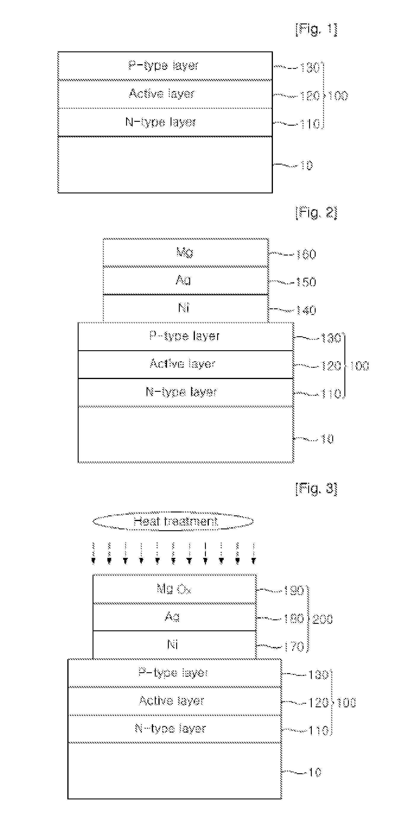
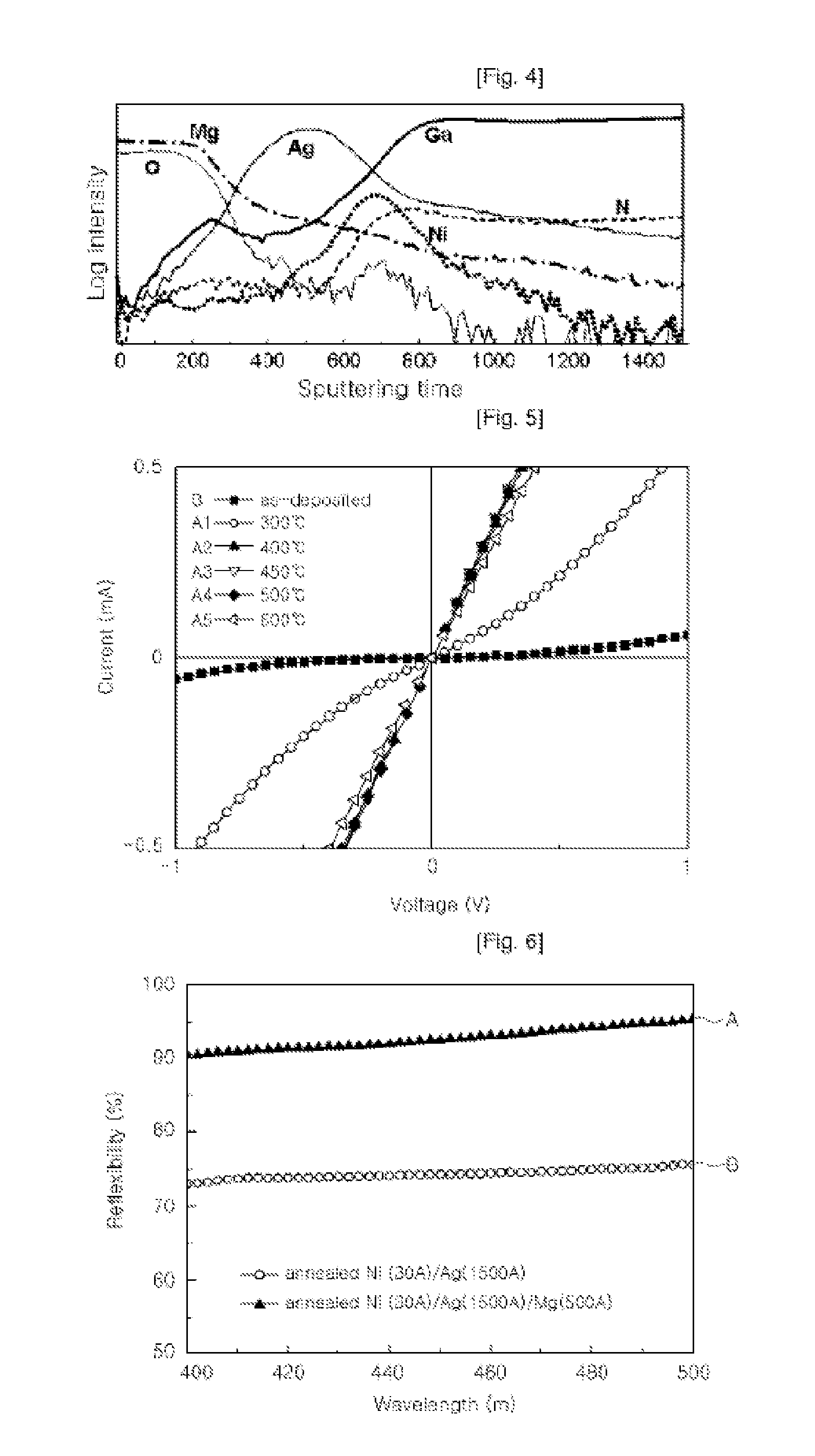
[0039]FIGS. 1 to 3 are sectional views illustrating a method of forming an ohmic electrode according to the present invention.

[0040]Referring to FIG. 1, if a substrate 10 is provided, a predetermined semiconductor layer 100 is formed thereon.

[0041]The substrate 10 may be SiC, Si, ZnO, GaAs or gallium phosphide (GaP) substrate. The sapphire substrate is more preferably used as the substrate.

[0042]The semiconductor layer 100 may be formed of films including one of Si, GaN, AN, InGaN, AlGaN, AlInGaN and combinations including at least one of the foregoing. For example, in this embodiment, an n-type layer 110 is formed by implanting n-type dopants into a GaN film, an active layer 120 with a multiple quantum well structure is formed by alternately growing GaN films, as barrier layers, and InGaN films, as quantum well layers, on the n-type layer. And a p-type layer 130 is formed by growing a GaN film again and then implanting p-type dopants thereinto. At this time, a buffer layer (not sho...

second embodiment

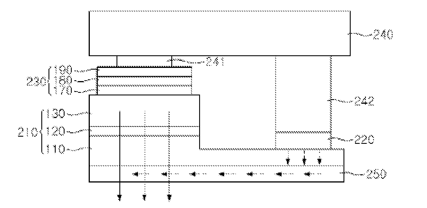
[0060]FIG. 8 is a sectional view showing a semiconductor light emitting element with a flip-chip structure according to the present invention.

[0061]Referring to FIG. 8, the semiconductor light emitting element includes a semiconductor layer 210 with a multi-layered structure having an n-type layer 110, an active layer 120 and a p-type layer 130. The semiconductor light emitting element also includes an n-type electrode 220 formed in a predetermined region of the n-type layer 110; a p-type electrode 230 formed on top of the p-type layer 130; a submount substrate 240 connected to the two electrodes 220 and 230 using bumps 241 and 242; and a current diffusion layer 250 formed under the n-type layer 110.

[0062]The n-type layer 110, the active layer 120 and the p-type layer 130 may be formed, respectively, by depositing layers including one selected from the group consisting of Si, GaN, AN, InGaN, AlGaN, AlInGaN and combinations at least one of the foregoing. Each of the n-type and p-type...

third embodiment

[0070]FIG. 9 is a sectional view showing a semiconductor light emitting element with a vertical structure according to the present invention.

[0071]Referring to FIG. 9, the semiconductor light emitting element includes a semiconductor layer 310 with a multi-layered structure having an n-type layer 110, an active layer 120 and a p-type layer 130. The semiconductor light emitting element also includes an n-type electrode 320 formed on the n-type layer 110, and a p-type electrode 330 formed under the p-type layer 130. Here, the p-type electrode 330 includes a bonding layer170, a semiconductor layer 180 and a protective layer 190. That is, it is preferred to use the ohmic electrode described in the previous embodiment.

[0072]A method of fabricating the semiconductor light emitting element with such a configuration will be described as follows.

[0073]An n-type layer 110, an active layer 120 and a p-type layer 130 are sequentially laminated on a mother substrate (not shown) to form a semicon...


PUM


Abstract

The present invention relates to a method of forming an ohmic electrode in a semiconductor light emitting element, comprising: forming a semiconductor layer having a light emitting structure on a substrate, sequentially laminating a bonding layer, a reflective layer and a protective layer on the semiconductor layer, and forming an ohmic electrode by performing a heat treatment process to form ohmic bonding between the semiconductor layer and the bonding layer and to form an oxide film on at least a portion of the protective layer; and a semiconductor light emitting element using the ohmic electrode. According to the present invention, since a reflective layer is formed of Ag, Al and an alloy thereof with excellent light reflectivity, the light availability is enhanced. Further, since contact resistance between a semiconductor layer and a bonding layer is small, it is easy to apply large current for high power.

Description

CROSS REFERENCE TO RELATED APPLICATIONS[0001]This application is a divisional of application Ser. No. 12 / 296,356, filed on Oct. 7, 2008, which is the National Stage of International Application No. PCT / KR07 / 001,898, filed on Apr. 18, 2007, and claims priority from and the benefit of Korean Patent Application No. 10-2006-0035088, filed on Apr. 18, 2006, which are all hereby incorporated by reference for all purposes as if fully set forth herein.BACKGROUND OF THE INVENTION[0002]1. Field of the Invention[0003]The present invention relates to a method of forming an ohmic electrode and a semiconductor light emitting element, and more particularly, to a method of forming an ohmic electrode formed on a semiconductor layer to allow a current applied thereto, and a semiconductor light emitting element using the ohmic electrode.[0004]2. Discussion of the Background[0005]Semiconductor light emitting elements have advantages of small size, lightweight, low power consumption and long life span, ...

Claims


Application Information

Patent Timeline
Patent Type & Authority Applications(United States)
IPC IPC(8): H01L33/60H01L33/00H01L33/32H01L33/40
CPCH01L33/0095H01L33/405H01L33/32
Inventor LEE, JONG-LAM
Owner SEOUL VIOSYS CO LTD
Why Eureka
Try Eureka