Semiconductor wafer

Inactive Publication Date: 2011-09-01
LEXTAR ELECTRONICS CORP
View PDF8 Cites 0 Cited by
  • Summary
  • Abstract
  • Description
  • Claims
  • Application Information

AI Technical Summary

Benefits of technology

[0011]The present invention relates to a semiconductor wafer, which can prevent bowing of the semiconductor wafer during an epitaxial growth process so as to enhance quality of the semiconductor wafer.
[0018]The semiconductor wafer of the present invention includes the separating structure, so a stress that is accumulated in the semiconductor stacked layer structure during an epitaxial growth process can be released. Consequently, bowing of the semiconductor wafer can be reduced, and thus, quality of the semiconductor wafer can be enhanced.

Problems solved by technology

However, the semiconductor wafer should be induced to bow, and quality of the semiconductor wafer is degraded in a process of manufacturing the above-mentioned light-emitting diode, because of different thermal expansion coefficient and lattice constant between the substrate and the stacked structure, and an accumulated stress in the stacked structure during the epitaxial growth process.
Consequently, wavelengths of light emitted by the light-emitting diodes on the same semiconductor wafer should be non-uniformity.

Method used


Image

  • Semiconductor wafer
  • Semiconductor wafer
  • Semiconductor wafer

Examples


fourth embodiment

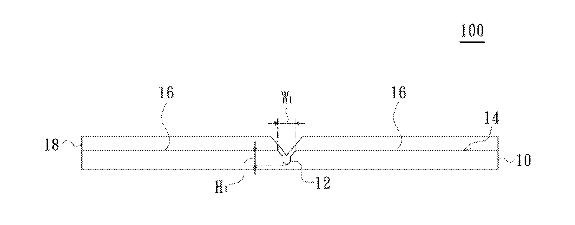
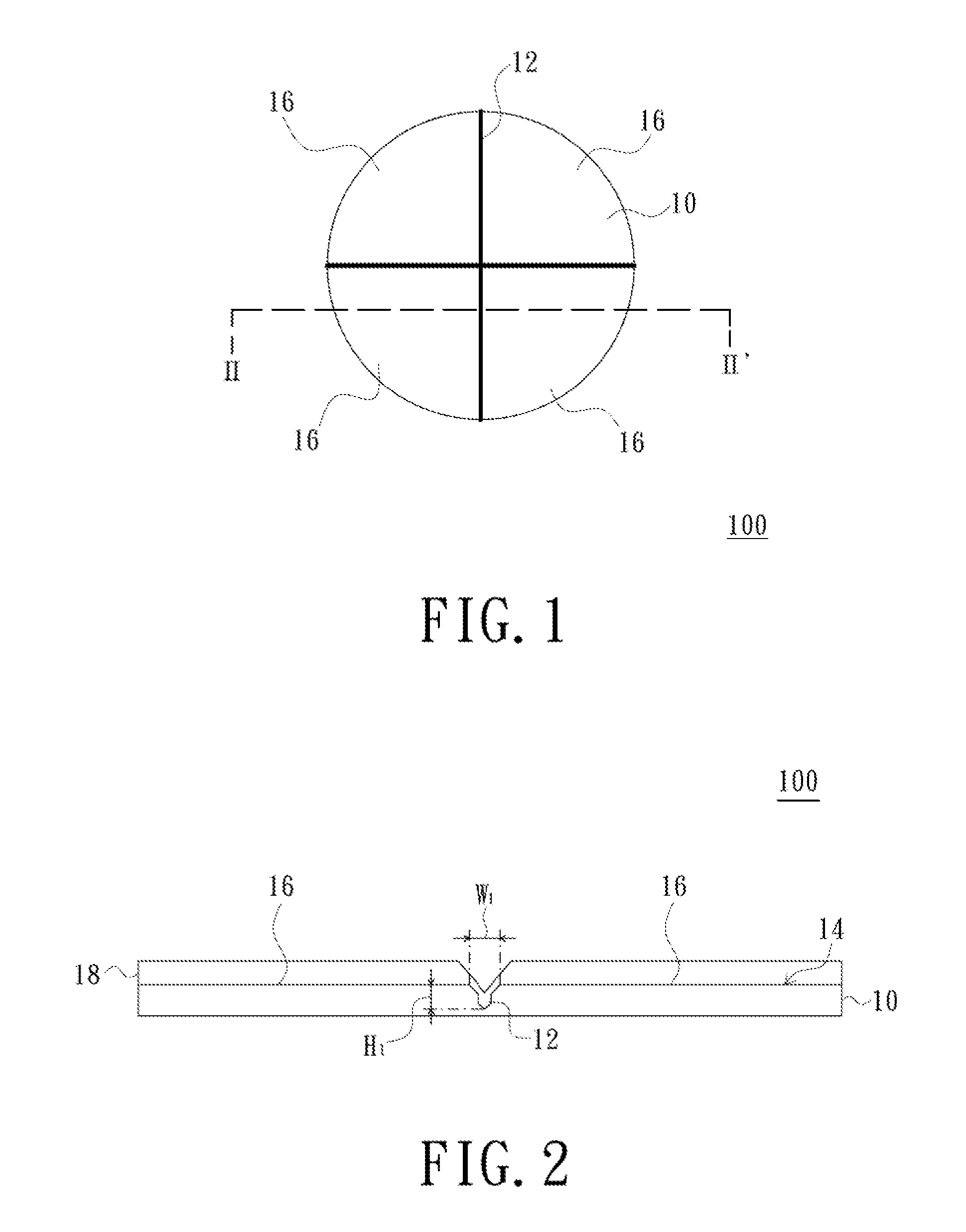
[0049]It should be understood that, the separating structure can also be formed on a surface of the substrate that is away from the semiconductor stacked layer structure. FIG. 9 is a side cross-sectional view of a semiconductor wafer according to the present invention. Referring to FIG. 9, a semiconductor wafer 300 includes a substrate 30, at least one separating structure 34 and a semiconductor stacked layer structure 36. The substrate 30 has a first surface 32 and a second surface 32′. The separating structure 34 is formed on the second surface 32′. The semiconductor stacked layer structure 36 is disposed on the first surface 32. The separating structure 34 can be a trench or a protrusion. In the embodiment, the separating structure 34 is the trench. A structure and a manufacturing method of the separating structure 34 can be the same or similar to that of the separating structure of the above embodiments, and material of the semiconductor stacked layer structure 36 can be the sam...

fifth embodiment

[0050]In addition, the separating structures can also be formed on the two surface of the substrate. FIG. 10 is a side cross-sectional view of a semiconductor wafer according to the present invention. Referring to FIG. 10, a semiconductor wafer 400 includes a substrate 40, at least one first separating structure 44, at least one second separating structure 44′ and a semiconductor stacked layer structure 46. The substrate 40 has a first surface 42 and a second surface 42′. The first separating structure 44 is formed on the first surface 42. The second separating structure 44′ is formed on the second surface 42′. The semiconductor stacked layer structure 46 is disposed on the first surface 42 and the first separating structure 44. The first separating structure 44 or the second separating structure 44′ can be a trench or a protrusion. In the embodiment, the first separating structure 44 is the protrusion, and the second separating structure 44′ is the trench. A structure and a manufac...


PUM


Abstract

A semiconductor wafer includes a substrate, a first separating structure and a semiconductor stacked layer structure. The substrate has a first surface. The first separating structure is formed on the first surface to divide the first surface into a plurality of independent regions. The minimum area of each of the regions is more than or equal to one square inch. The semiconductor stacked layer structure is disposed on the first surface and the first separating structure. The semiconductor wafer can prevent bowing of the semiconductor wafer during an epitaxial growth process so as to enhance quality of the semiconductor wafer.

Description

CROSS-REFERENCE TO RELATED APPLICATION[0001]This application claims the priority benefit of Taiwan application serial no. 099105863, filed on Mar. 1, 2010. The entirety of the above-mentioned patent application is incorporated herein by reference and made a part of this specification.BACKGROUND[0002]1. Technical Field[0003]The present invention relates to a semiconductor wafer, and more particularly relates to a semiconductor wafer with a relatively large size.[0004]2. Description of the Related Art[0005]Recently, various electronic components are manufactured from semiconductor wafers, such as a light-emitting diode.[0006]The light-emitting diode has advantages of small size, long lifetime, low driving voltage, low power consumption, rapid response and good oscillation-proof, and has been widely used in electronic products, such as cars, computers, communication products or other consumer electronic products.[0007]The semiconductor wafer of the light-emitting diode includes a subst...

Claims


Application Information

Patent Timeline
IPC IPC(8): H01L33/00H01L23/00
CPCH01L33/007H01L33/20H01L33/12
Inventor CHEN, FU-BANGFANG, KUO-LUNGHUANG, KUN-FUWANG, TE-CHUNG
Owner LEXTAR ELECTRONICS CORP
Why Eureka
Try Eureka