Multi inductively coupled plasma reactor and method thereof

a plasma reactor and inductive coupling technology, applied in the direction of electrical discharge tubes, decorative surface effects, electrical apparatus, etc., can solve the problems of contaminated interior of the reactor, non-uniform plasma density, deformation or damage of the electrode, etc., and achieve the effect of enhancing process efficiency

Inactive Publication Date: 2011-08-25
GENERAL CO LTD
View PDF8 Cites 34 Cited by
  • Summary
  • Abstract
  • Description
  • Claims
  • Application Information

AI Technical Summary

Benefits of technology

[0010]Accordingly, it is an object of this invention to provide a multi-inductively coupled plasma reactor and method thereof, capable of enhancing process efficiency with respect to a large scale substrate to be processed by forming uniform plasma on the large area using a central plasma source and a peripheral source.
[0011]It is an another object of this invention to provide a multiple gas supplier and a plasma reactor, capable of enhancing process efficiency with respect to a large scale substrate to be processed by forming uniform plasma on the large area using process gas provided multiply and central plasma source and peripheral plasma source.
[0033]Further, it is possible to form an independent multiple plasma area without electrical interference in the plasma reactor using the interference prevention electrode grounded between the central plasma source and the peripheral plasma source.

Problems solved by technology

However, when a capacitive coupling electrode becomes large scale in order to process large scale substrates to be processed, the electrode is deformed or damaged due to the deterioration of the electrode.
In this case, the electric filed intensity becomes non-uniformed so that the plasma density may be non-uniformed and the interior of reactor may be contaminated.
In also the case of the inductive coupled plasma source, it is not easy to obtain an uniform plasma density like the case of making the area of an inductive coil antenna large
There also exist the problems described above in such semiconductor manufacturing processes using laser.
The large scale production equipment increases entire equipment area, resulting in increase of production cost.
Further, due to the large scale substrate to be processed, there occurs a problem that central area and peripheral area of the substrate to be processed are not processed uniformly by plasma.
That is, since plasma forms centered on the central area of the substrate to be processed compared with the peripheral area, there occurs a difficulty that the substrate to be processed is processed entirely and uniformly.

Method used


Image

  • Multi inductively coupled plasma reactor and method thereof
  • Multi inductively coupled plasma reactor and method thereof
  • Multi inductively coupled plasma reactor and method thereof

Examples


Embodiment Construction

[0049]To fully understand many objects to be accomplished by various embodiments and operational advantages of this invention, preferred embodiments of this invention will be described in a more detailed manner with reference to the attached drawings. In the attached drawings, like elements will be referred to as like numerals. Furthermore, the detailed technical explanation of already known functions and constructions will be omitted herein to avoid a faint determination of the subject matter of this invention.

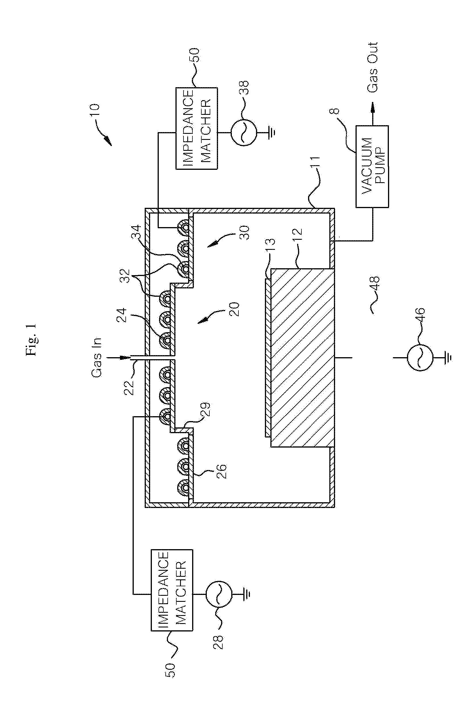
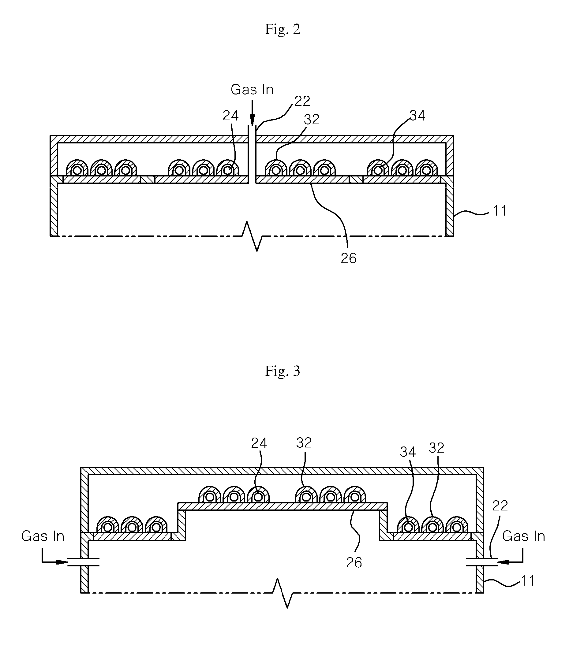
[0050]FIG. 1 is a sectional view showing a plasma process apparatus in which a central plasma source and a peripheral plasma source are separated each other according to a preferred embodiment of the invention.

[0051]Referring to FIG. 1, a multi-inductively coupled plasma reactor 10 according to a preferred embodiment of the invention is constructed of a reactor body 11, a central plasma source 20 and a peripheral plasma source 30. The reactor body 11 internally has a substrat...


PUM

PropertyMeasurementUnit
frequencyaaaaaaaaaa
frequencyaaaaaaaaaa
frequencyaaaaaaaaaa

Abstract

Disclosed is a multi-inductively coupled plasma reactor and method thereof. In a multi-inductively coupled plasma reacting method, an etching method to increase a specific portion of a substrate to be processed includes etching a specific portion of a substrate to be processed; and depositing a passivation layer on a surface of the specific portion etched, wherein the etching and depositing steps are repeatedly proceeded, and one of both steps is executed when there is plasma formed by a central plasma source and a peripheral plasma source. According to the multi-inductively coupled plasma reactor and method thereof of the invention, it is possible that plasma is uniformly processed on the entire area of the substrate since the central plasma source and the peripheral source are provided separately. Further, it is possible to form an independent multiple plasma area without electrical interference in the plasma reactor using the interference prevention electrode grounded between the central plasma source and the peripheral plasma source. Further, the plasma formed by the central plasma source and the peripheral plasma source is used to deeply etch a specific portion of the substrate to be processed.

Description

BACKGROUND OF THE INVENTION[0001]1. Field of the Invention[0002]The invention relates to a multi-inductively coupled plasma reactor and method thereof, and in particular to a method to deeply etch a specific portion of a substrate to be processed using a multi-inductively coupled plasma.[0003]2. Description of the Prior Art[0004]In the silicon anisotropic etching method, processes of etching a specific portion of substrate to be processed and depositing a passivation layer on the specific portion etched are repeatedly performed. The specific portion of the substrate to be processed is etched in a desired depth while the etching and depositing processes are repeatedly performed. Such etching and depositing processes are accomplished by plasma.[0005]Plasma is highly ionized gas including the same number of positive ions and electrons. Plasma discharge is used to excite gas in order to generate activated gas including ions, free radicals, atoms and molecules. The activated gas is widel...

Claims


Application Information

Patent Timeline
Patent Type & Authority Applications(United States)
IPC IPC(8): C23F1/00C23F1/08
CPCH01J37/321H01J37/32449H01J37/32165H01J37/3211
Inventor HUH, NO-HYUNKIM, GYOO-DONGNAM, CHANG-WOOPARK, SUNG-MINCHOI, DAE-KYU
Owner GENERAL CO LTD
Why Eureka
Try Eureka