
ESD protection device

The ESD protection device uses BJTs and specific geometric configurations to enhance ESD performance in deep submicron semiconductor processes, addressing worsening ESD tolerance by uniformly discharging currents and reducing parasitic capacitance, achieving higher current sustainability and lower trigger voltages.

Active Publication Date: 2011-08-18
UNITED MICROELECTRONICS CORP
View PDF5 Cites 2 Cited by
  • Summary
  • Abstract
  • Description
  • Claims
  • Application Information

AI Technical Summary

Benefits of technology

The solution effectively improves ESD performance by uniformly discharging currents in multiple directions, reducing parasitic capacitance, and maintaining robustness with smaller device sizes, as demonstrated by higher current sustainability and lower trigger voltages in human body model tests compared to conventional devices.

Problems solved by technology

ESD is the main factor of electrical overstress (EOS) which causes damage to most of electronic devices or systems.
Such damage can result in the permanent damage of semiconductor devices and computer systems, so that the circuit function of integrated circuits (ICs) is affected and the operation of electronic products is abnormal.
In a deep submicron semiconductor process, the ESD tolerance is getting worse as dimensions of the IC devices are getting miniaturized.

Method used


Image

  • ESD protection device
  • ESD protection device
  • ESD protection device

Examples


first embodiment

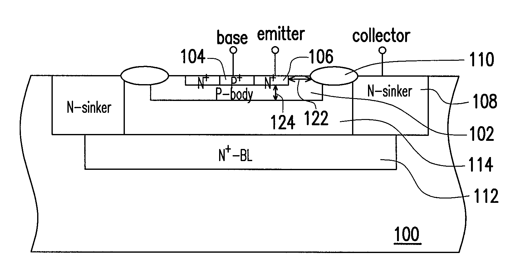
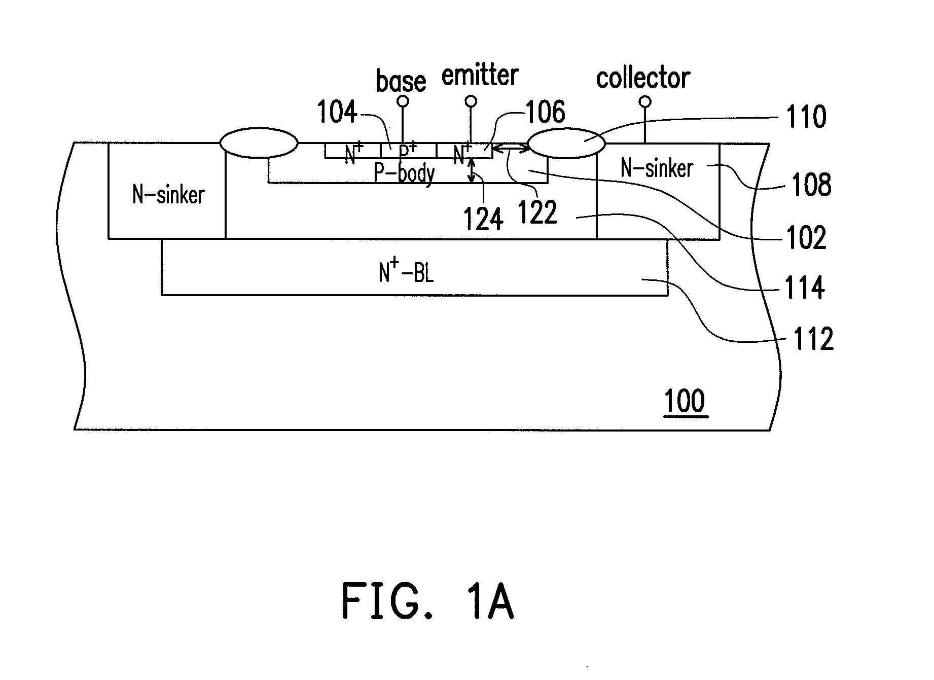
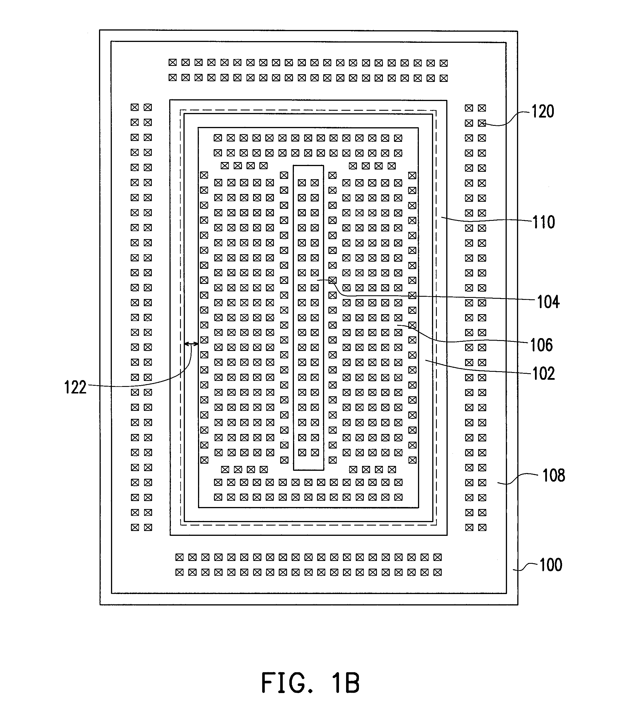
[0035]Referring concurrently to FIGS. 1A and 1B, the ESD protection device of the first embodiment is deployed in a substrate 100. The substrate 100 is, for example, a P-type substrate, and an N-epitaxial layer 114 may be configured therein. The ESD protection device includes a P-body region 102, a P-type doped region 104, an N-type doped region 106, an N-sinker region 108, an N-buried layer 112 and an isolation structure 110.

[0036]The P-body region 102 is configured in the substrate 100 within the N-epitaxial layer 114. The P-type doped region 104, such as a P+ doped region, is configured in the P-body region 102. The P-type doped region 104 can be deployed in the middle of the P-body region 102. The N-type doped region 106, such as an N+ doped region, is configured in the P-body region 102 and surrounds the P-type doped region 104. The N-type doped region 106 may adjoin the profile of the P-type doped region 104. The P-type doped region 104 and the N-type doped region 106, for exa...

second embodiment

[0049]Alternatively, the ESD protection device can be further modified so as to apply to other semiconductor processes. FIG. 4 depicts schematically, in a cross-sectional diagram, the ESD protection device according to the present invention.

[0050]Referring to FIG. 4, the ESD protection device of the second embodiment is deployed in a substrate 400, such as a P-type substrate or a deep N-well region. The ESD protection device includes a first P-type doped region 402, a second P-type doped region 404, a first N-type doped region 406, a second N-type doped region 408 and an isolation structure 410.

[0051]The first P-type doped region 402 is configured in the substrate 400. The second P-type doped region 404, such as a P+ doped region, is configured in the first P-type doped region 402. The second P-type doped region 404 can be deployed in the middle of the first P-type doped region 402. The first N-type doped region 406, such as an N+ doped region, is configured in the first P-type dope...


PUM


Abstract

An ESD protection device is described, which includes a P-body region, a P-type doped region, an N-type doped region and an N-sinker region. The P-body region is configured in a substrate. The P-type doped region is configured in the middle of the P-body region. The N-type doped region is configured in the P-body region and surrounds the P-type doped region. The N-sinker region is configured in the substrate and surrounds the P-body region.

Description

CROSS-REFERENCE TO RELATED APPLICATION[0001]This application is a continuation application of and claims priority benefits of U.S. patent application Ser. No. 12 / 469,164, filed on May 20, 2009, now allowed. The entirety of the above-mentioned patent application is hereby incorporated by reference herein and made a part of this specification.BACKGROUND OF THE INVENTION[0002]1. Field of the Invention[0003]The present invention relates to a semiconductor device, and in particular, to an electrostatic discharge (ESD) protection device.[0004]2. Description of Related Art[0005]ESD is the main factor of electrical overstress (EOS) which causes damage to most of electronic devices or systems. Such damage can result in the permanent damage of semiconductor devices and computer systems, so that the circuit function of integrated circuits (ICs) is affected and the operation of electronic products is abnormal. Accordingly, a number of methods have been developed to protect the semiconductor IC ...

Claims


Application Information

Patent Timeline
Patent Type & Authority Applications(United States)
IPC IPC(8): H01L29/73
CPCH01L27/0259H01L29/735H01L29/0692H10D89/711H10D62/126H10D10/60
Inventor CHAO, FANG-MEI
Owner UNITED MICROELECTRONICS CORP
Learn More