Optical Sensor

a technology of optical sensors and optical holograms, applied in the field of optical sensors, can solve the problems of inability to reproduce the effect of normal means, inability to customize objects by embossed holograms, and disadvantages of authenticity checking by means of microscopes, and achieve the effect of reducing costs and shortening tim

Inactive Publication Date: 2011-07-21
BAYER INTELLECTUAL PROPERTY GMBH
View PDF12 Cites 8 Cited by
  • Summary
  • Abstract
  • Description
  • Claims
  • Application Information

AI Technical Summary

Benefits of technology

[0079]The use of the sensor according to the invention affords the advantage that identification and / or authentication of an object can be performed by machine or supported by machine and enables a quantitative assessment of the probability with which an object corresponds to an asserted object. Machine performance or support permits the checking of a larger number of objects on the basis of their characteristic reflection patterns in a shorter time and with lower costs than a (purely) person-based performance e.g. with the aid of a microscope as described in DE102007044146A1. Furthermore, machine performance or machine support permits a comparison of reflection patterns which were authenticated at different times. The tracking of objects (track and trace) is thereby made possible.

Problems solved by technology

Such effects cannot be reproduced by means of the normal and widespread copying and printing techniques.
What is disadvantageous, however, is that security elements produced in this way always have the same embossed hologram.
Secondly, objects cannot be individualized by the embossed holograms on account of the indistinguishability thereof.
What is disadvantageous about checking authenticity by means of a microscope is the high outlay.
A combination of features for product tracking and for protection against forgery is afforded by RFID chips, but the latter can be used only to a limited extent on account of their comparatively high costs, slow read-out speed and sensitivity to electromagnetic interference fields.

Method used


Image

  • Optical Sensor
  • Optical Sensor
  • Optical Sensor

Examples


Embodiment Construction

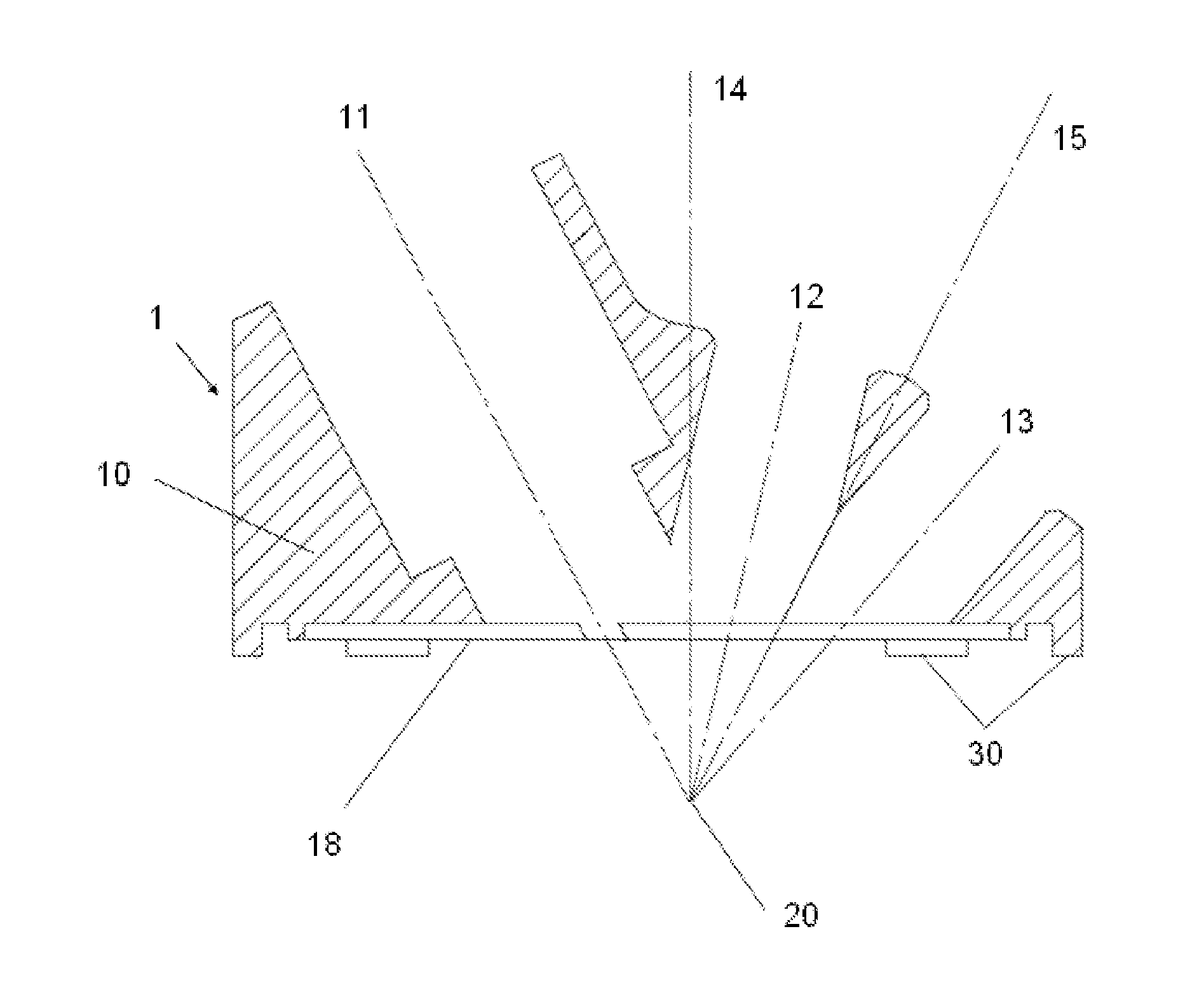
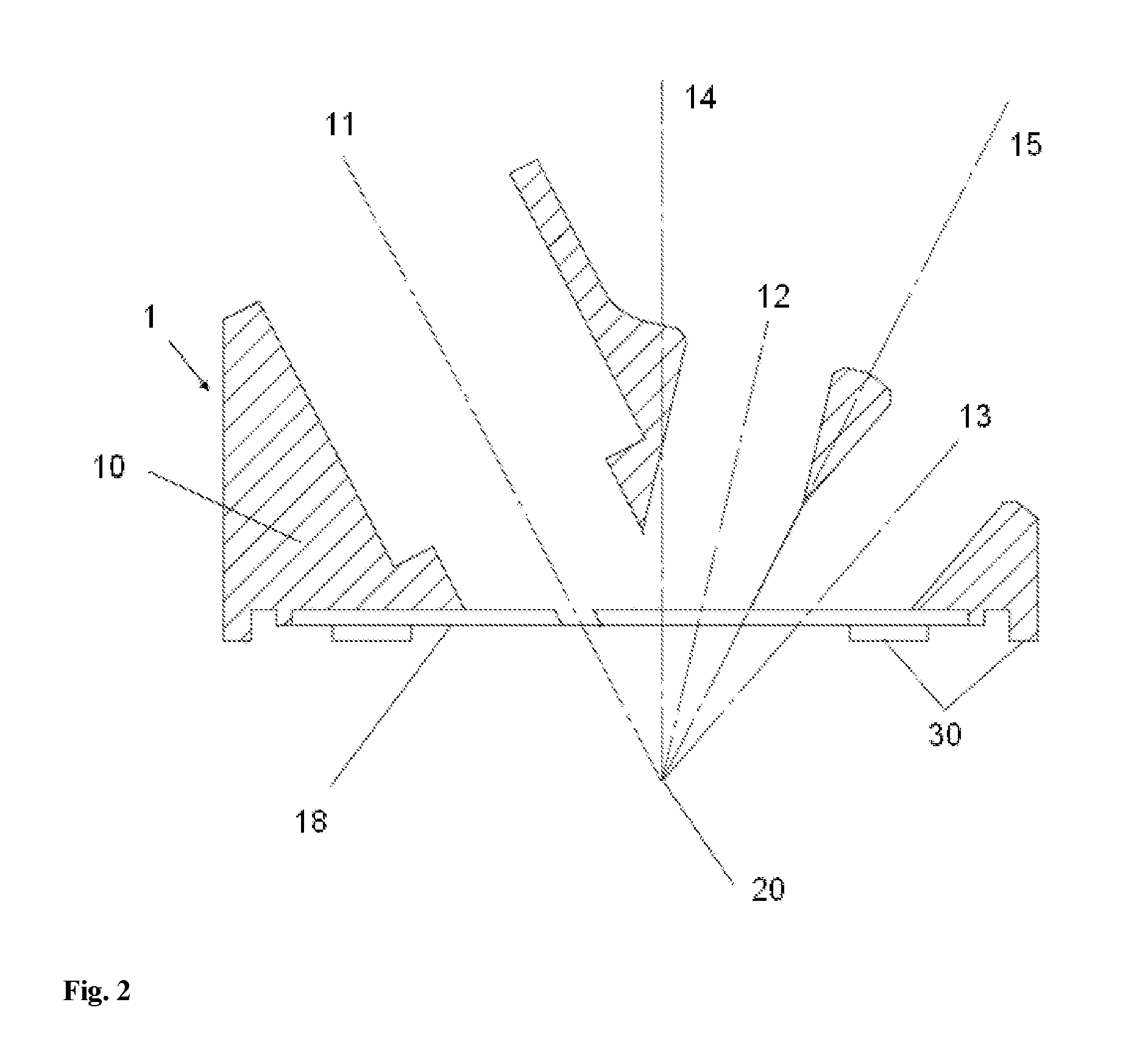
[0088]FIGS. 1a and 2b show a sensor 1 according to the invention without optical components in a perspective illustration. FIG. 2 shows the sensor 1 from FIGS. 1a and 1b in cross section.

[0089]The central element of the sensor 1 is formed by a block 10, which is preferably embodied in one or two pieces and which serves for receiving all the optical components of the sensor according to the invention.

[0090]Optical components are understood to mean all components of the sensor which are arranged in the beam path between radiation source and photodetector, including the laser and the photodiodes themselves. Optical elements form a selection of the optical components; they serve for beam shaping and focussing. In particular, lenses, diaphragms, diffractive optical elements and the like are referred to as optical elements.

[0091]The optical block 10 comprises an identified outer surface 18, which is directed at the object during the detection of characteristic reflection patterns of said ...


PUM

PropertyMeasurementUnit
angleaaaaaaaaaa
thicknessaaaaaaaaaa
distanceaaaaaaaaaa

Abstract

The invention relates to an optical sensor for detecting characteristic reflection patterns caused by randomly distributed and/or oriented microreflectors. The invention furthermore relates to the method od using a sensor according to the invention for identifying and/or authenticating objects.

Description

[0001]This is an application filed under 35 USC §371 of PCT / EP2009 / 002809, claiming priority to DE 10 2008 051 409.8 filed on Oct. 11, 2008.BACKGROUND OF THE INVENTION[0002](1) Field of the Invention[0003]The invention relates to an optical sensor for detecting characteristic reflection patterns caused by randomly distributed and / or oriented microreflectors. The invention furthermore relates to the use of a sensor according to the invention for identifying and / or authenticating objects.[0004]For protection against forgery, identity cards, banknotes, products, etc. are nowadays provided with elements which can be copied only with special knowledge and / or high technical outlay. Such elements are referred to here as security elements. Security elements are preferably connected inseparably to the objects to be protected. An attempt to separate the security elements from the object preferably leads to their destruction, in order that the security elements cannot be misused.[0005]The auth...

Claims


Application Information

Patent Timeline
Patent Type & Authority Applications(United States)
IPC IPC(8): G01N21/47G07D7/12
CPCB42D2035/50G06K19/086B42D25/328B42D25/29G07D7/121G01J1/10G07D7/12G01N21/00
Inventor GERIGK, MARKUSBACKER, ANDREASBIRSZTEJN, THOMASIMHAUSER, RALFROTH, CHRISTIANSPETH, WALTERVOUGIOUKAS, SIMON
Owner BAYER INTELLECTUAL PROPERTY GMBH
Why Eureka
Try Eureka