
Photostructured Mechanical Devices and Methods for Making Same

a mechanical device and photostructure technology, applied in the field of photostructured ceramics, can solve the problems of device not working as well in two dimensions, device is then susceptible to damage, device is prone to damage, and risk destroying fragile devices

Inactive Publication Date: 2011-07-14
THE AEROSPACE CORPORATION
View PDF17 Cites 9 Cited by
  • Summary
  • Abstract
  • Description
  • Claims
  • Application Information

AI Technical Summary

Benefits of technology

[0011]The methods enable the three-dimensional fabrication of complex components that are sealed within a ceramic material. Advantageously, while the structures and the three-dimensional interconnects are delicately fashioned with aspect ratios that can exceed 50:1, these fragile integrated units are contained in a block of electrically insulating glass or ceramic material that can have the shape of a die or have the convenient dimensions of a chip carrier package. The volume becomes the package, which not only insulates the embedded devices or structures, but also allows for ease of handling without causing damage to small devices.
[0012]The method allows for the design and true three-dimensional fabrication of structures that could have feature sizes down to 50 microns or less (for some commercially made photostructural glasses or ceramics) and an overall size scaling to square meters or larger. Furthermore, the invention also allows the possibility for fabricating stacked arrays of electrically conducting microstructures for microinstrument applications. Regardless of the specific nature of the device fabricated, the resulting part is encapsulated in a glass or ceramic medium volume that is resistant to the natural environment, to many caustic chemicals, and can operate at elevated temperatures. These and other advantages will become more apparent from the following detailed description.

Problems solved by technology

However, some devices do not work as well in two dimensions, such as high frequency antennas and transformers.
However, the repetitive two-dimensional approach works well for laying out multilevel conducting lines, but has limitations when more complex three-dimensional electrical conducting structures are to be fashioned, such as with coils, inductors, and horn antennas where curvature is used to enhance efficiency.
These approaches may risk destroying the fragile device as a result of surface tension forces during the drying phase, such as with induced stresses.
If the device survives the drying phase, the device is then susceptible to damage during the instrument development phase when the structure or device must be inserted or placed onto the platform by an automated pick and place machine.
The potential for damage is also present when these fragile small devices are connected, such as by wire bonding and soldering, to an adjoining electrical unit using an electrical interface.
However, a problem with such encapsulation is a required number of housing components integrated as a singular housing.
The encapsulation problem is similar to plastic injection machines where the two halves of a mold are pressed together, and hot plastic is injected through an injection port and conduit runners to cavities defining a desired plastic part.
The prior photostructurable manufacturing processes do not provide a processing approach by which delicate structures and devices can be disposed in the volume for enabling functional interconnections fashioned within a protective volume.

Method used


Image

  • Photostructured Mechanical Devices and Methods for Making Same
  • Photostructured Mechanical Devices and Methods for Making Same
  • Photostructured Mechanical Devices and Methods for Making Same

Examples


Embodiment Construction

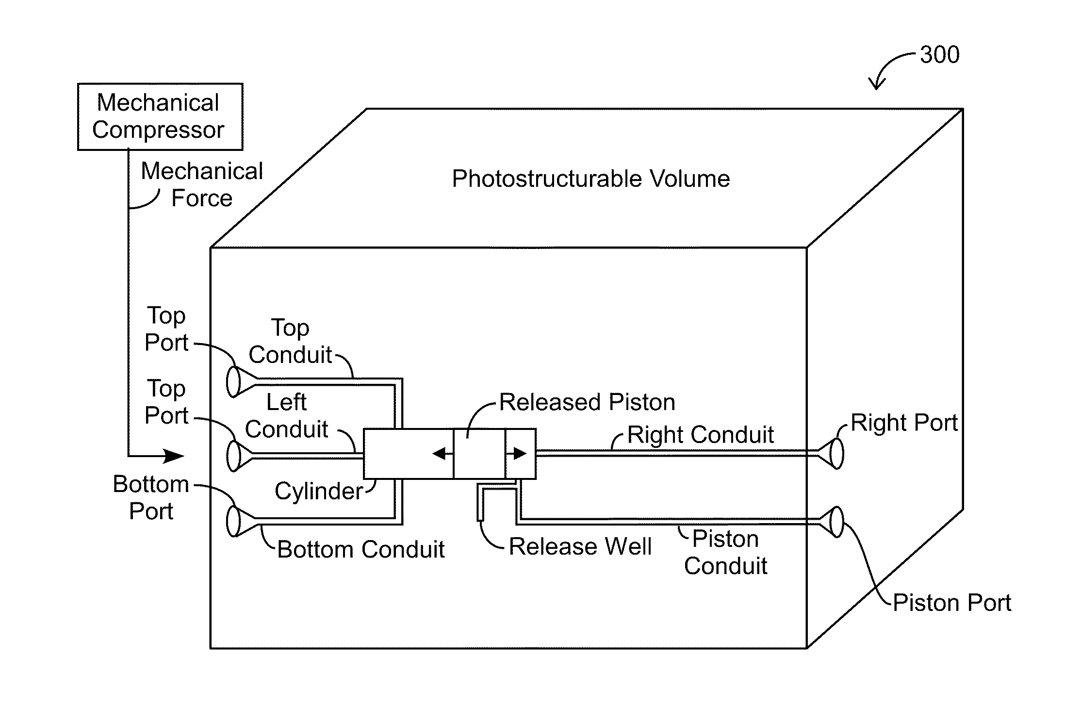
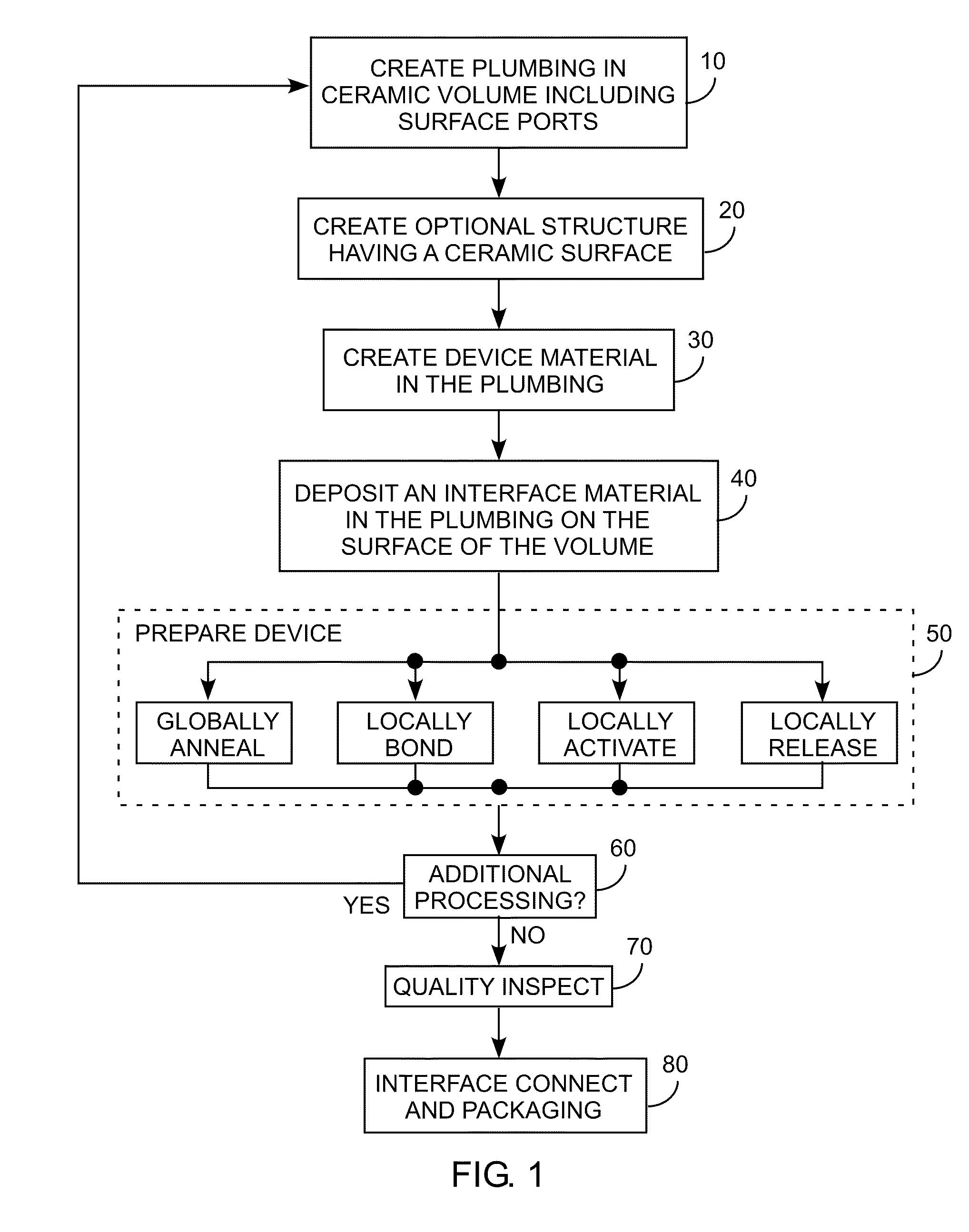
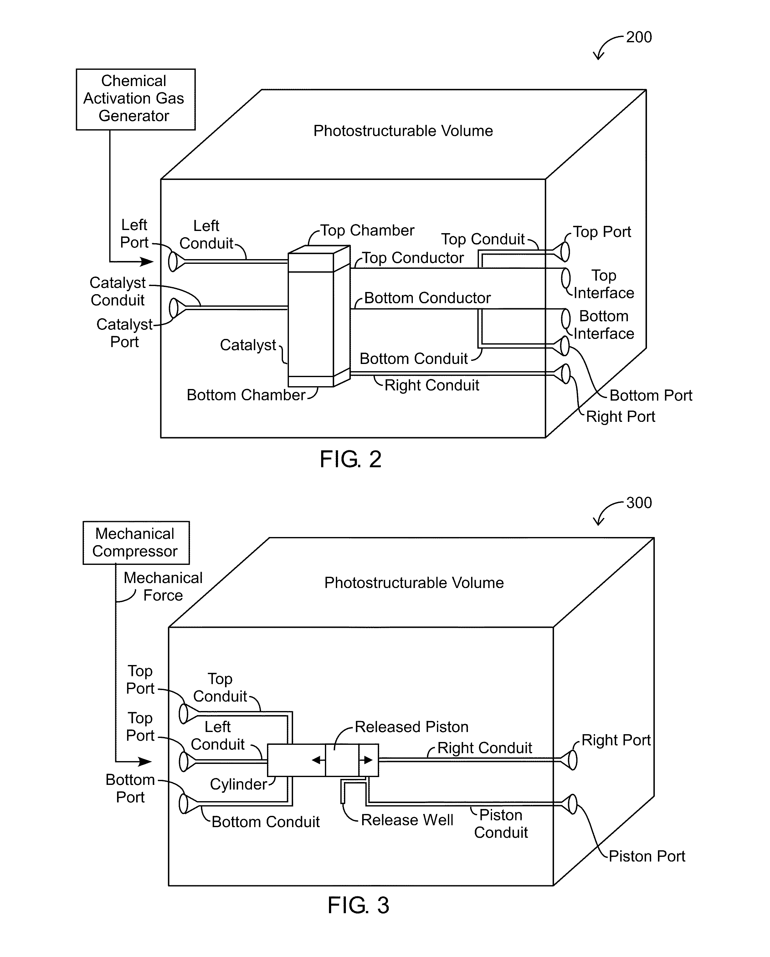
[0021]An embodiment of the invention is described with reference to the figures using reference designations as shown in the figures. Referring to FIG. 1, block 10, a three dimensional (3D) volume of photostructurable glass or ceramic material is first processed by laser exposure to define plumbing within the 3D volume. The plumbing can take any desired cavity shape and can be oriented in any direction, such as in vias, tanks, voids, gaps, spheres, tunnels, bubbles, tubes, conduits, plates, coils, feedthroughs, guides, and apertures, among many other possible vacated structures.

[0022]The plumbing can include vacated portions that do not function as mere conduits, but as optional cavities performing a desired function, as described in block 70. For example, a tank can be used as an operational receptacle for any operational device material during operational use. The volumes can be processed for creating internal empty volumes that then become internal operational structures, such as...


PUM

PropertyMeasurementUnit
sizeaaaaaaaaaa
temperatureaaaaaaaaaa

Abstract

A photostructurable ceramic is processed using photostructuring process steps for embedding devices within a photostructurable ceramic volume, the devices may include one or more of chemical, mechanical, electronic, electromagnetic, optical, and acoustic devices, all made in part by creating device material within the ceramic or by disposing a device material through surface ports of the ceramic volume, with the devices being interconnected using internal connections and surface interfaces.

Description

REFERENCE TO RELATED APPLICATIONS[0001]The present application is related to the following co-pending applications: “Photostructured Chemical Devices and Methods for Making Same,” application Ser. No. ______, filed Jan. 13, 2010; “Photostructured Electrical Devices and Methods for Making Same,” application Ser. No. ______, filed Jan. 13, 2010; “Photostructured Magnetic Devices and Methods for Making Same,” application Ser. No. ______, filed Jan. 13, 2010; “Photostructured Optical Devices and Methods for Making Same,” application Ser. No. ______, filed Jan. 13, 2010; and “Photostructured Acoustic Devices and Methods for Making Same,” application Ser. No. ______, filed Jan. 13, 2010. The entirety of each aforementioned application is hereby incorporated by reference.FIELD OF THE INVENTION [0002]This invention generally relates to the fields of photostructurable ceramics. More particularly, the inventions relate to devices disposed in photostructurable ceramic volumes and methods for m...

Claims


Application Information

Patent Timeline
Patent Type & Authority Applications(United States)
IPC IPC(8): F16M11/00B23P11/00
CPCB81B2201/051B81B2203/0338Y10T29/49826Y10T74/22B81C1/00634
Inventor HELVAJIAN, HENRY
Owner THE AEROSPACE CORPORATION
Learn More