
Multiple resonance antenna, manufacturing method therefor and communication device

a technology of multi-resonance antennas and manufacturing methods, applied in the direction of resonant antennas, waveguide type devices, elongated active element feeds, etc., can solve the problems of shortened physical length and deteriorating radiation characteristics of high-frequency antenna electrodes

Inactive Publication Date: 2011-06-23
TDK CORPARATION
View PDF6 Cites 17 Cited by
  • Summary
  • Abstract
  • Description
  • Claims
  • Application Information

AI Technical Summary

Benefits of technology

[0012]An object of the present invention is to provide a low-cost multiple resonance antenna which can keep a balance between high-frequency antenna characteristics and low-frequency antenna characteristics while achieving miniaturization, a manufacturing method therefor, and a communication device using the same.
[0015]Since the multiple resonance antenna according to the present invention has a structure that the first and second antenna electrodes whose one ends are connected to each other are disposed together on the dielectric substrate, as described above, miniaturization and cost reduction can be effectively achieved as compared with the above multilayered one.
[0017]In the multiple resonance antenna according to the present invention, when the first antenna electrode is used as the low-frequency antenna electrode and the second antenna electrode is used as the high-frequency antenna electrode, the high-dielectric part having a high permittivity is disposed beneath a part of the first antenna electrode including a free end and having a maximum magnetic field strength. Hence, the first antenna electrode can ensure a necessary electrical length with having few bends.
[0018]In addition, since the high-dielectric part is disposed beneath said part of the first antenna electrode, it hardly affects radiation characteristics of the second antenna electrode. Thus, the second antenna electrode can ensure an effective bandwidth.
[0019]Therefore, the multiple resonance antenna according to the present invention can achieve a balance between the high-frequency antenna characteristics and the low-frequency antenna characteristics.
[0021]In the method for manufacturing the multiple resonance antenna according to the present invention, outsert molding or insert molding is used for formation of the dielectric substrate, so that the dimensional deviation can be reduced as compared with the case where individual parts are separately formed and then joined together, making it possible to properly reduce unevenness such as a difference in level that may be created at a border between the high-dielectric part and the other part. This effectively prevents the reduction of the yield of the product and therefore reduces the cost.

Problems solved by technology

However, although this solution can ensure an effective electrical length for the low-frequency antenna electrode, radiation characteristics may be deteriorated by the bend.
With this structure, however, there is a problem of deteriorating radiation characteristics of the high-frequency antenna electrode.
This is because the physical length of the high-frequency antenna electrode is extremely shortened, narrowing the effective bandwidth.
In this case, therefore, antenna characteristics of the high-frequency antenna electrode are deteriorated as compared with those of the low-frequency antenna electrode, causing an imbalance of antenna characteristics between the low-frequency one and the high-frequency one.
Even with this structure, however, since the high-frequency antenna electrode is covered with the dielectric substrate for the low-frequency antenna electrode, it is also impossible to avoid deterioration of radiation characteristics of the high-frequency antenna electrode.
In addition, disposing the two antenna electrodes on different dielectric layers results in increasing the overall thickness to prevent miniaturization and also requiring a through-hole between the layers to reduce the yield and increase the cost.

Method used


Image

  • Multiple resonance antenna, manufacturing method therefor and communication device
  • Multiple resonance antenna, manufacturing method therefor and communication device
  • Multiple resonance antenna, manufacturing method therefor and communication device

Examples


Embodiment Construction

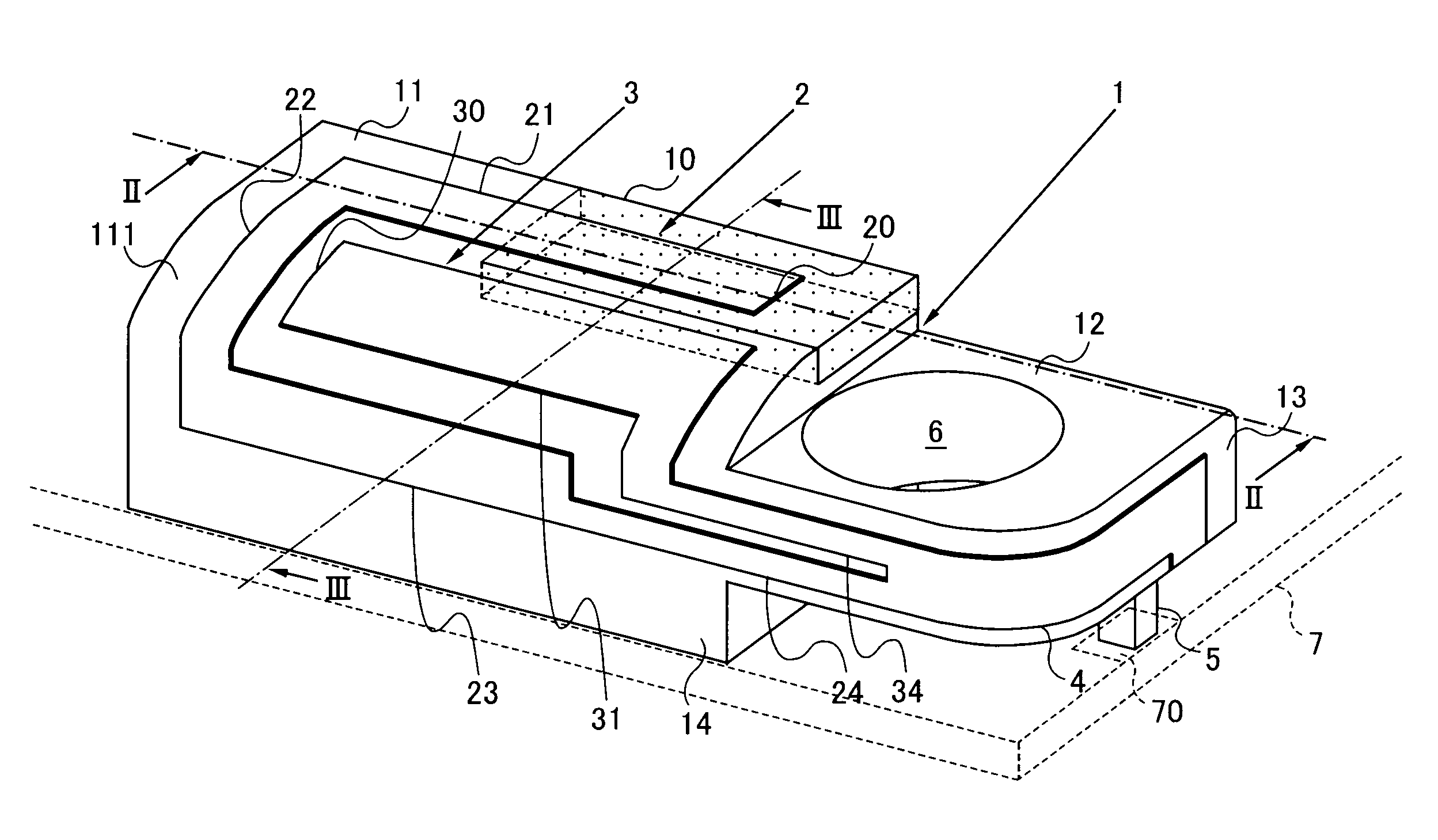
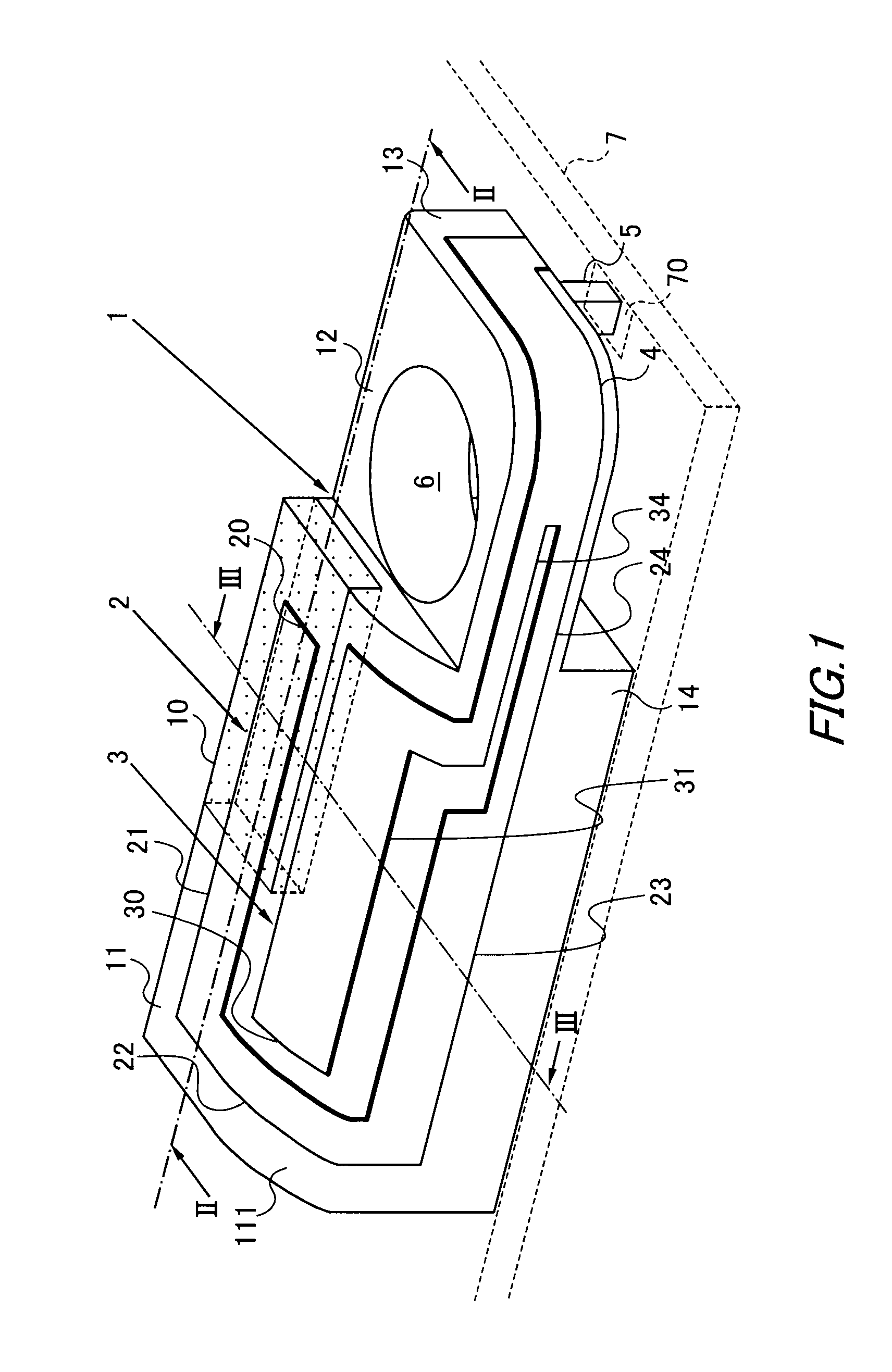
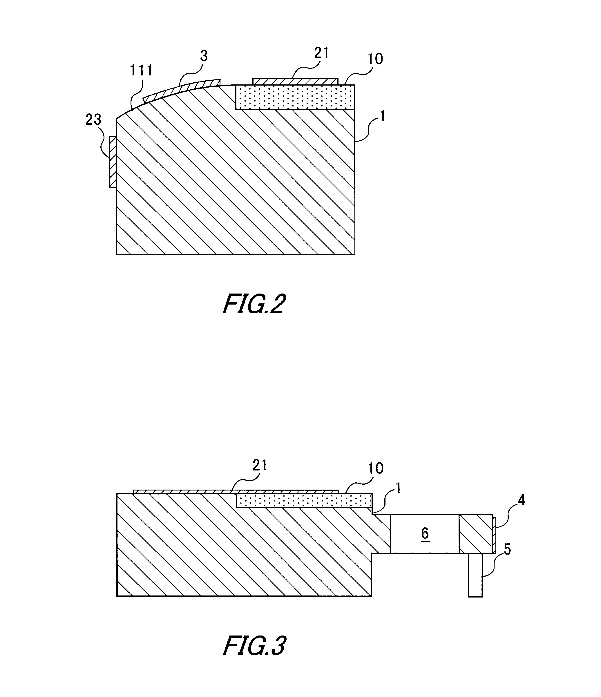
[0033]Referring to FIGS. 1 to 3, a multiple resonance antenna according to the present invention includes a dielectric substrate 1, a first antenna electrode 2 and a second antenna electrode 3 disposed together on the dielectric substrate 1, a power feeding electrode 4, and a connection electrode 5. It should be noted that the multiple resonance antenna in the figure is illustrated as being mounted on a circuit board 7 represented by dotted lines, for convenience.

[0034]The dielectric substrate 1 is preferably made of a composite dielectric material being a mixture of a synthetic resin and dielectric ceramic powder. For example, the synthetic resin may be ABS (acrylonitrile butadiene styrene) resin or PC (polycarbonate) resin. The dielectric ceramic powder may be barium titanate series ceramic powder or titanium oxide series ceramic powder. Advantageously, the use of such a composite dielectric material makes it possible to adjust the relative permittivity of the dielectric substrate...


PUM

PropertyMeasurementUnit
Lengthaaaaaaaaaa
Dielectric polarization enthalpyaaaaaaaaaa
Flexibilityaaaaaaaaaa

Abstract

A multiple resonance antenna includes a dielectric substrate, a first antenna electrode and a second antenna electrode, the first and second antenna electrodes being disposed together on the dielectric substrate with first ends connected to each other but with second ends remaining free, the dielectric substrate including a high-dielectric part having a higher relative permittivity than another part, the high-dielectric part being disposed beneath a part of the first antenna electrode including the second end.

Description

BACKGROUND OF THE INVENTION[0001]1. Field of the Invention[0002]The present invention relates to a multiple resonance antenna, a manufacturing method therefor, and a communication device using the same.[0003]2. Description of the Related Art[0004]A multiple resonance antenna includes two antenna electrodes of different resonance frequencies per one element and therefore can deal with different two frequency bands even though it is a single element. Typically, the antenna electrodes are each formed as a λ / 4 monopole antenna and branch off from a common power feeding path. Examples of devices to which the multiple resonance antenna is applicable include a mobile communication device having both functions of GPS (global positioning system) and Bluetooth (which is a registered trademark, though not mentioned again), such as a mobile phone. GPS utilizes radio waves of 1.57 GHz band, while Bluetooth utilizes radio waves of 2.45 GHz band, so that the multiple resonance antenna has to be ab...

Claims


Application Information

Patent Timeline
IPC IPC(8): H01Q1/38H01P11/00H01Q5/10
CPCH01Q1/243H01Q1/38Y10T29/49016H01Q9/42H01Q21/30H01Q9/40
Inventor SOTOMA, NAOKISHIMODA, HIDEAKIURABE, JUNICHIROHIRABAYASHI, NORIYUKI
Owner TDK CORPARATION
Learn More