Method for depositing a transparent conductive oxide (TCO) film on a substrate and thin-film solar cell

a technology of conductive oxide and substrate, which is applied in the direction of coating, vacuum evaporation coating, semiconductor devices, etc., can solve the problems of large-scale coating efficiency in continuous operation systems, irregular decrease of deposition rate, and process stability problems, so as to achieve significant change in the surface resistance of the tco layer, increase the haze value, and the effect of high haze valu

Inactive Publication Date: 2011-05-12
VON ARDENNE ANLAGENTECHNIK GMBH
View PDF8 Cites 6 Cited by
  • Summary
  • Abstract
  • Description
  • Claims
  • Application Information

AI Technical Summary

Benefits of technology

[0034]In a beneficial embodiment of the thin-film solar cell according to the invention, the TCO layer thereby has a distinct column-like crystallite structure. That makes a particularly beneficial light scattering possible which is reflected by a high haze value of this TCO layer without the surface resistance of the TCO layer being significantly changed, in particularly significantly increased.
[0035]In another embodiment of the thin-film solar cell, the TCO layer has a textured and / or roughened surface that again contributes to the increase of the haze value which as already mentioned can be determined experimentally.
[0036]Using simple means, a thin-film solar cell can be manufactured at which the barrier layer consists of a SiOxNy or SiOx or SixNy with 0<x≦3 and 0<y≦4 with a high-level barrier effect against the diffusion of material from the substrate. The deposition of silicon-containing oxide and / or nitride materials is possible through various, known, simple and easy-to-control PVD methods. The manufacturing of the thin-film solar cell according to the invention can be further simplified if silicon-containing oxide and / or nitride materials are used for the seed layer so that this layer consists of SiOxNy or SiOx or SixNy layer with 0<x≦3 and 0<y≦4. Thereby, the barrier layer is optimized to the desired barrier effect while the seed layer is optimized to the morphological, electrical and optical properties of the on the seed layer deposited TCO layer. Thereto, the deposition conditions of the seed layer in comparison to the ones of the barrier layer are changed through choosing different process parameters, or choosing a respective course of these process parameters. Generally, it is possible that the seed layer of the thin-film solar cell according to the invention in a special embodiment has a gradual and / or abrupt change of its layer properties.

Problems solved by technology

However with adding the hydrogen, a regular decrease of the deposition rate is observed which presents itself as a disadvantage for an efficient coating on a large scale in continuous operation systems.
Additionally, the realization of the high frequency magnetron sputter (RF sputtering) of doped ZnO causes problems in regards to stability of the process, and thus, the layer homogeneity and in regards to the deposition rate.

Method used


Image

  • Method for depositing a transparent conductive oxide (TCO) film on a substrate and thin-film solar cell
  • Method for depositing a transparent conductive oxide (TCO) film on a substrate and thin-film solar cell
  • Method for depositing a transparent conductive oxide (TCO) film on a substrate and thin-film solar cell

Examples


Embodiment Construction

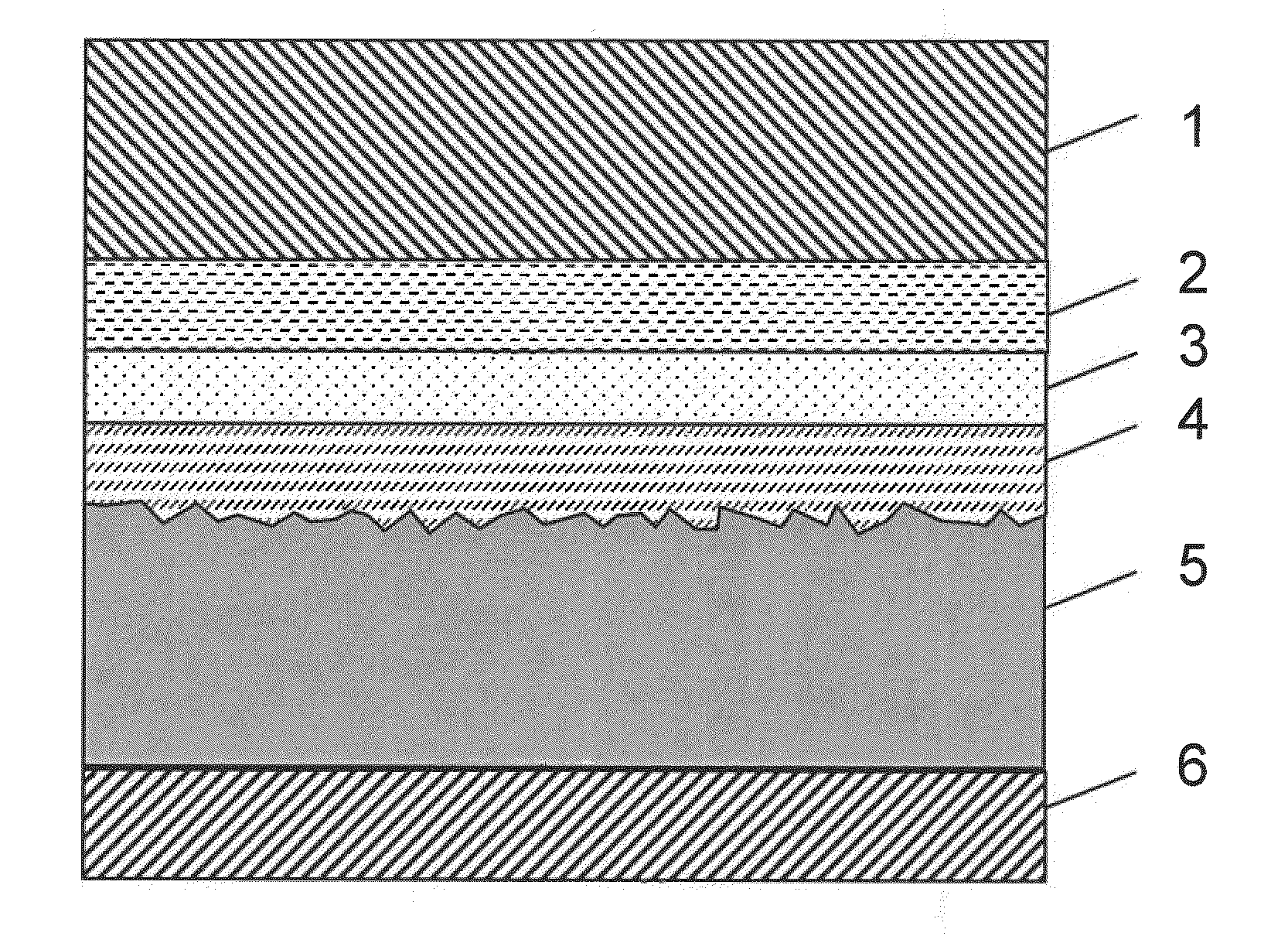
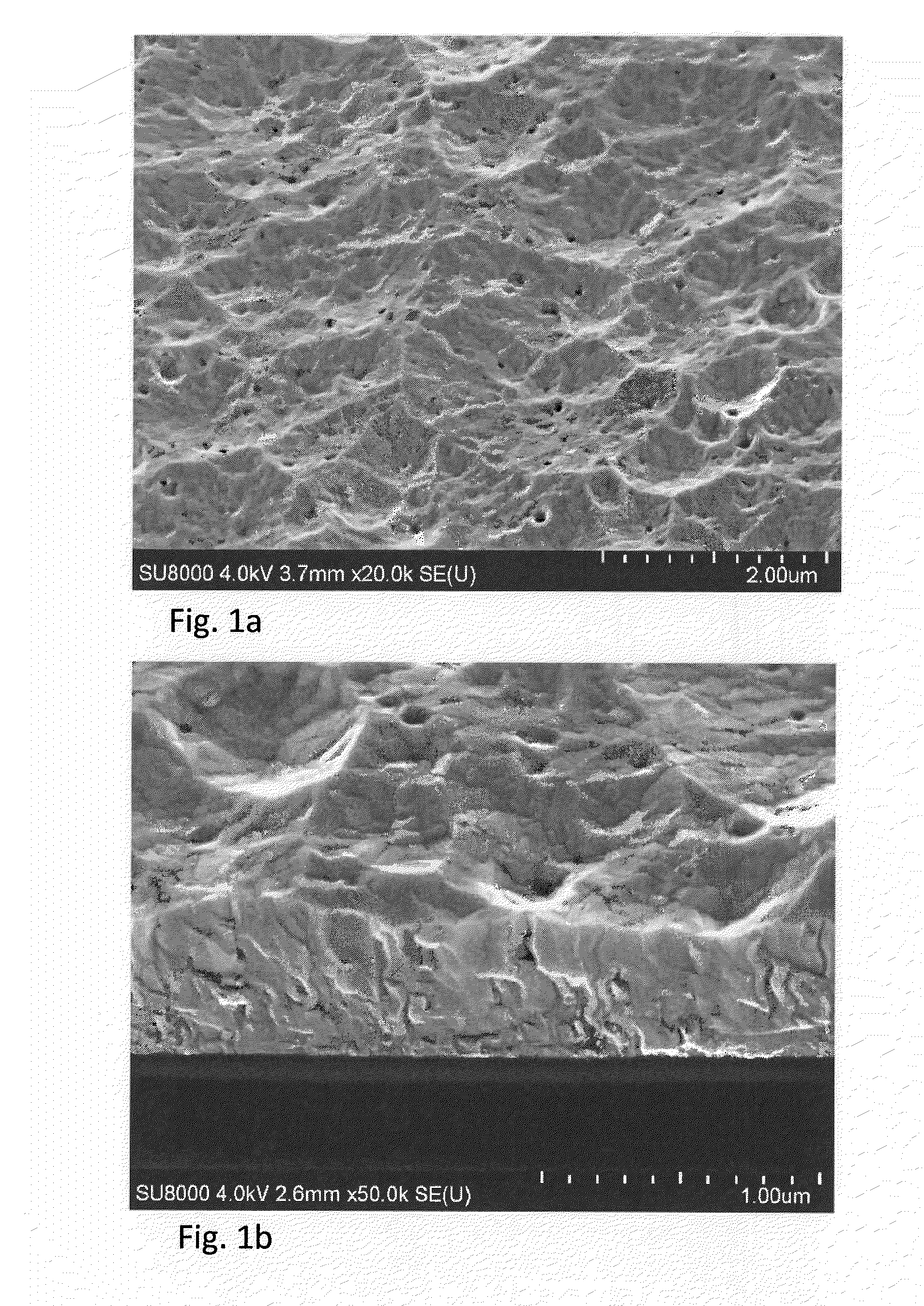
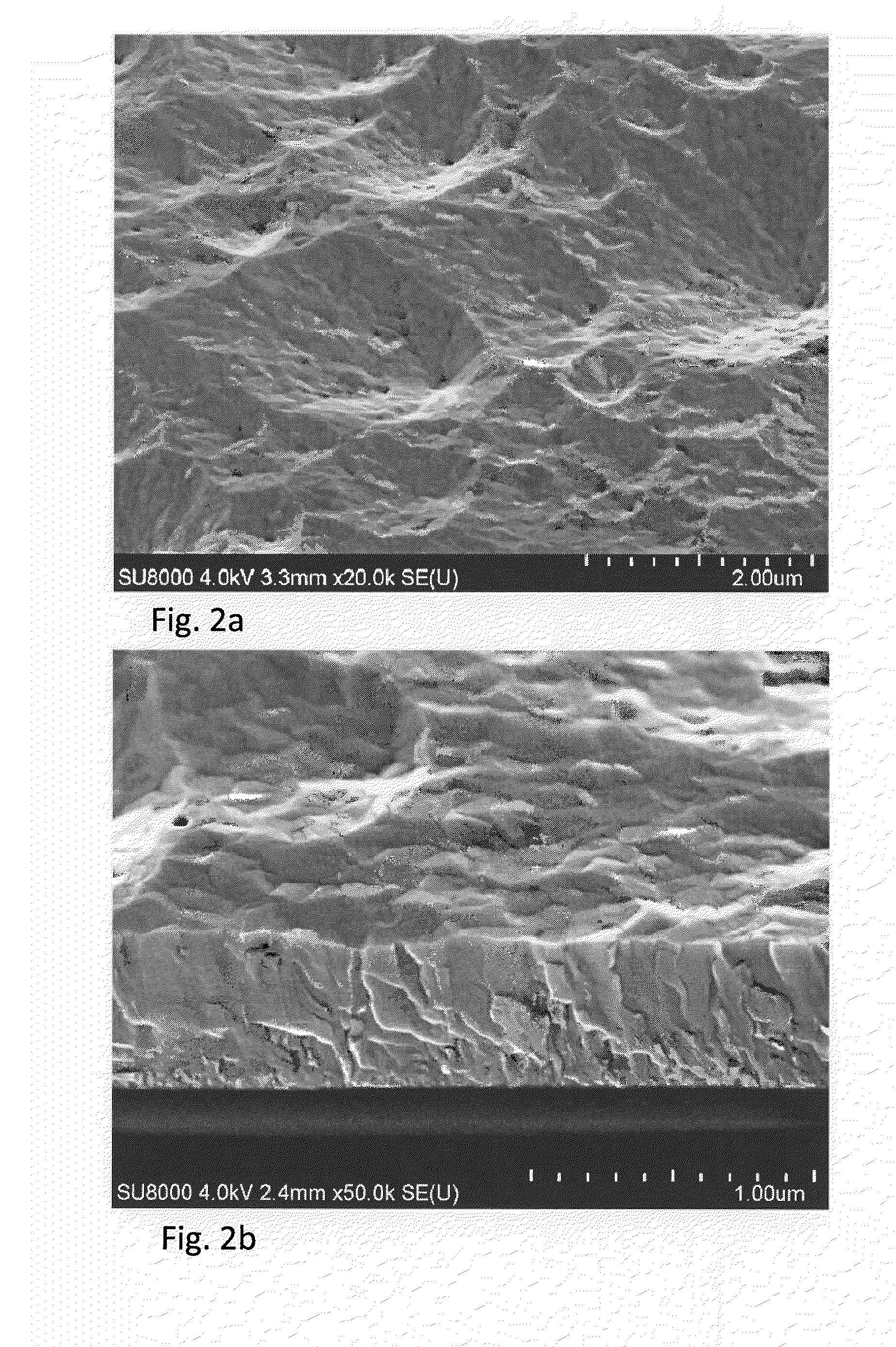
[0044]Both TCO layers of a similar thickness were deposited on a float glass substrate 1, on a silicon oxynitride barrier layer 2 and a silicon oxyntride seed layer 3. FIG. 1a shows the surface in 20,000-fold magnification and FIG. 1b shows a break through the layer stack in 50,000-fold magnification of the first TCO layer 4 which was deposited on a non-optimised seed layer 3, FIG. 2a and FIG. 2b show similar presentations of the second TCO layer 4 which was deposited on an optimised silicon oxynitride seed layer.

[0045]The directly on the float glass substrate 1 deposited dielectrical barrier layer 2 consists thereby in both instances of in the same conditions deposited sub-stiochiometric silicon oxynitride (SiOxNy). It operates as a barrier layer 2 for diffused sodium ions of the glasses in the layer system. With depositing of this barrier layer 2, the through the glass substrate additionally into the layer system introduced water can be removed from the substrate without this proc...


PUM

PropertyMeasurementUnit
frequenciesaaaaaaaaaa
temperaturesaaaaaaaaaa

Abstract

A method is provided for depositing a transparent conductive oxide (TCO) layer on a substrate, in which contaminations of the layers of the layer system is reduced through the diffusion of material from the substrate, and whose layer properties in respect to coupling and transmission of light are optimized. For that purpose, a barrier layer, a seed layer and a transparent conductive oxide layer are directly successively deposited on the substrate. Also, a thin-film solar cell is described which comprises such a transparent conductive oxide layer.

Description

BACKGROUND OF THE INVENTION[0001]The invention refers generally to a method for coating a substrate with a transparent conductive oxide layer, in the following designated as TCO layer, as well as a thin-film solar cell.[0002]The coating takes place on a substrate using physical vapor deposition (PVD method), usually through sputtering in a in-line method at which the substrate is moved through a coating chamber, and is then coated. For the sputtering, the substrate is moved passed a cathode assembly as coating source which has a target of the material that is to be deposited. Into the coating chamber, a working gas is introduced which has added a in comparison to the working gas small amount of hydrogen or other gases.[0003]Such conductive and transparent TCO layers can be used in various applications and in particular in the UV and in the IR range because of their optical properties, e.g. as a transparent electrode in thin-film solar cells or in flat screens, as a blocking layer in...

Claims


Application Information

Patent Timeline
Patent Type & Authority Applications(United States)
IPC IPC(8): H01L31/0216H01L31/0236
CPCC03C17/3435C03C2217/94C23C14/024Y02E10/50H01L31/0392H01L31/1884C23C14/086
Inventor DIMER, MARTINSCHOESSLER, TINAKNOTH, THOMASSTURM, RALFGRAUPNER, UWETHUMSCH, MARTINHECHT, HANS-CHRISTIAN
Owner VON ARDENNE ANLAGENTECHNIK GMBH
Why Eureka
Try Eureka