
Electron Beam Apparatus And Electron Beam Inspection Method

a technology of electron beam and electron beam, which is applied in the direction of material analysis using wave/particle radiation, material analysis by measuring secondary emission, instruments, etc., can solve the problem that the qualified image for inspection or measurement of a sample cannot be acquired in a short time, and the high elevation angle component at the generational position of the secondary particle cannot be sufficiently separated from the low-velocity component, etc. problem, to achieve the effect of enhanced shadow contras

Inactive Publication Date: 2011-05-05
HITACHI HIGH-TECH CORP
View PDF6 Cites 4 Cited by
  • Summary
  • Abstract
  • Description
  • Claims
  • Application Information

AI Technical Summary

Benefits of technology

Accordingly, an object of the present invention is to provide a charged-particle beam inspection technology capable of acquiring an image in which shadow contrast is more enhanced than a conventional one, in shorter time than that required conventionally.
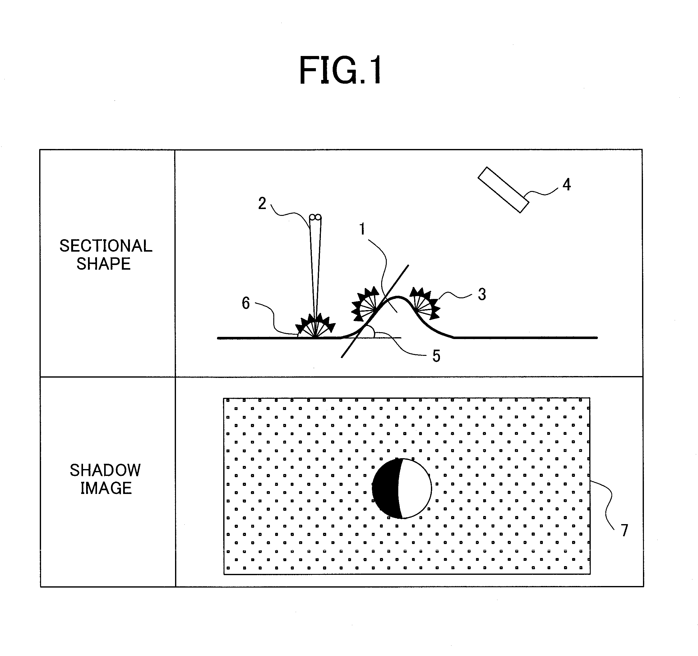
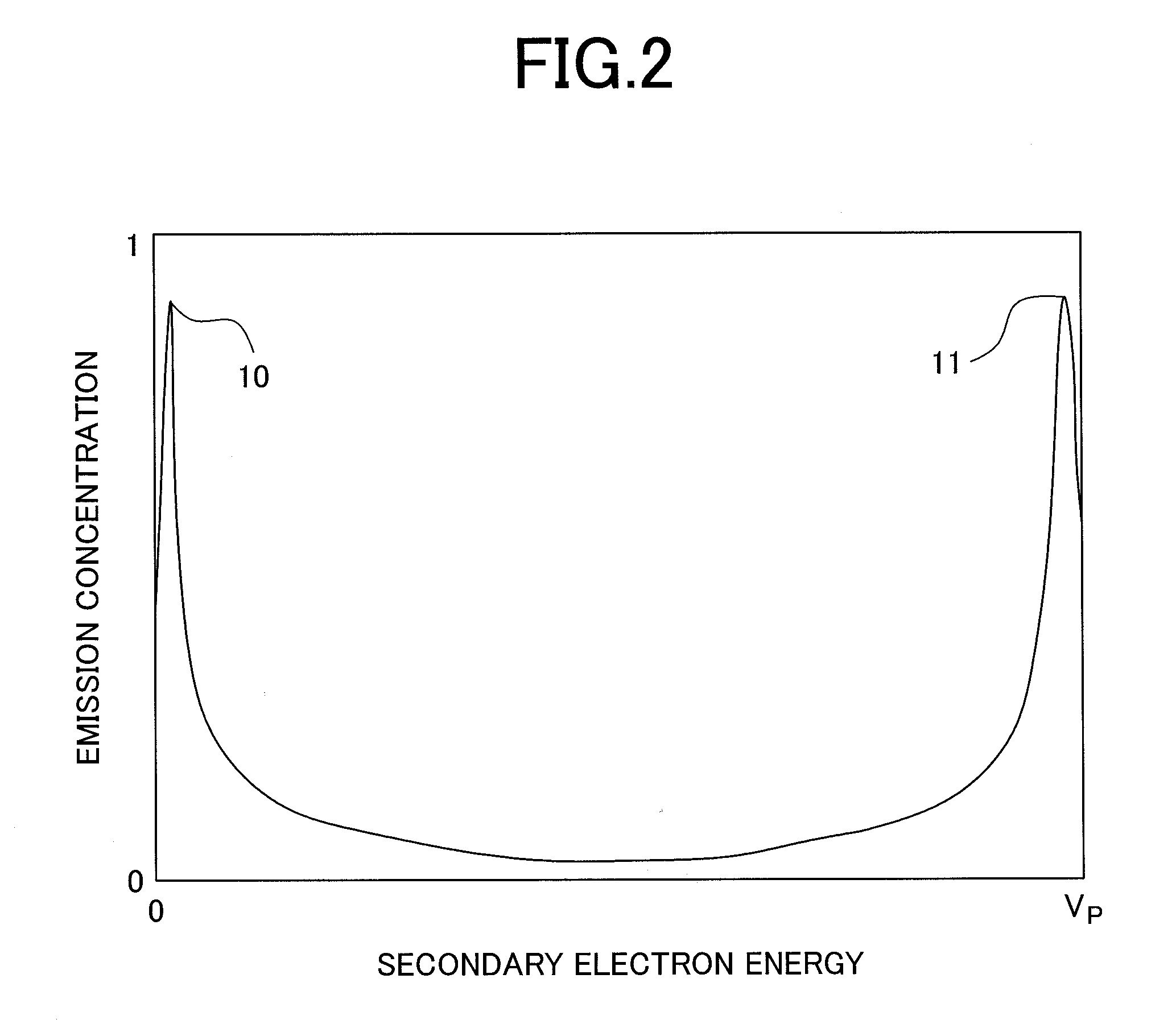
On the other hand, since the degree of the rotational angle of the backscattering electron 21 depending on the elevation angle is smaller than that of the secondary electron, a shadow contrast of an image produced based on the backscattering electron can be enhanced. Generally, the contrast of an observation image of a shallow roughness or a tiny foreign matter is weak. If the shallow roughness is observed in a way of enhancing the shadow, newly generated contrast is added to the shallow roughness, so that the contrast is enhanced. The newly generated contrast shall be referred to as a shadow contrast. Small rotational angle of a secondary particle enables to distinguish the azimuth angle component, thus the shadow contrast increases. Thus, by detecting a high-velocity component with a wide range in the elevation angle at a generational position, and distinguishing into the azimuth component, the shadow contrast is enhanced. Consequently, the shallow roughness or tiny foreign matter can be detected with high sensitivity.
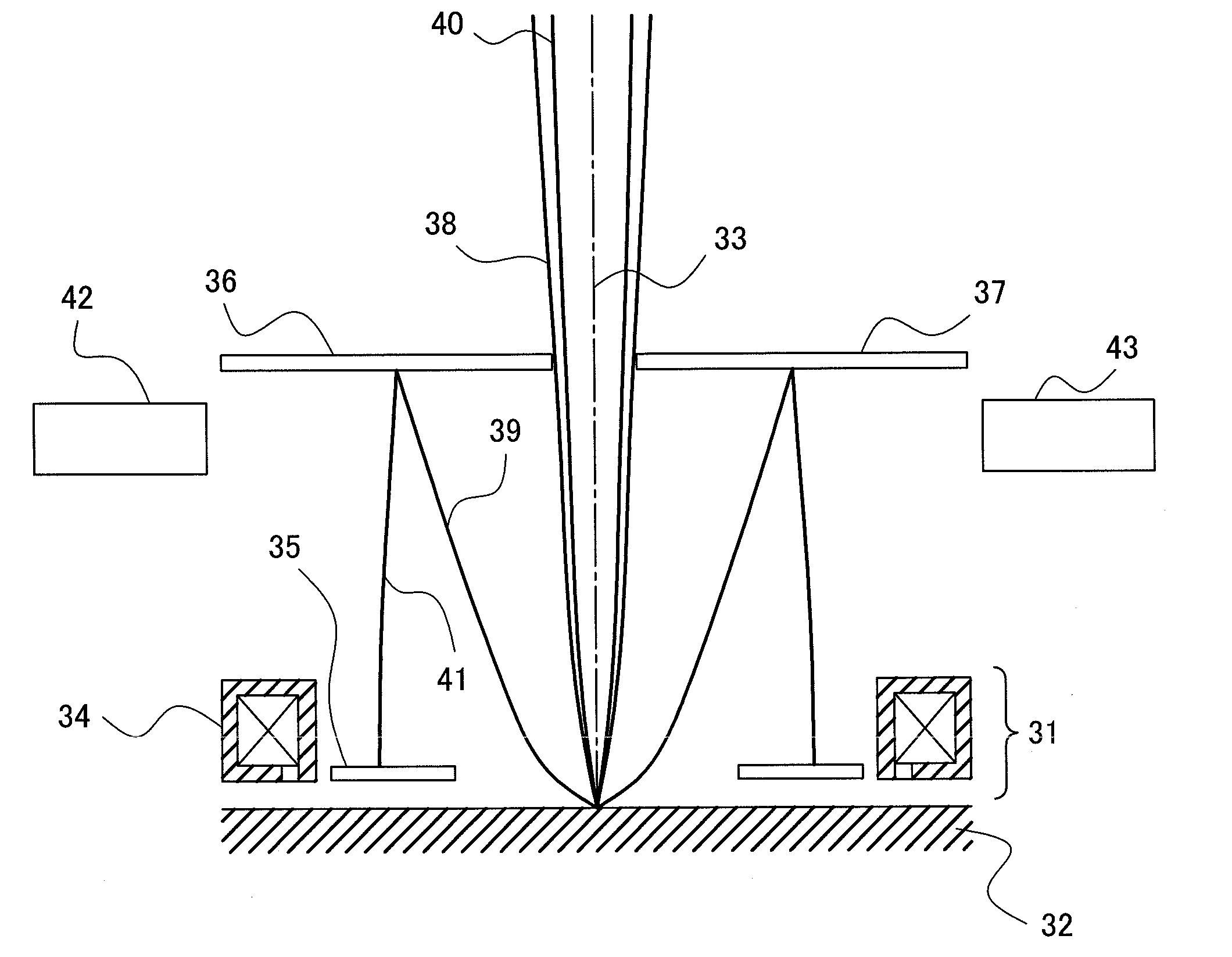
FIG. 5 shows the trajectory of a secondary particle in an electron optical system equipped with separation means for the high-velocity component and a low-velocity component of a secondary particle, more particularly, equipped with a trajectory separating means for a secondary electron and the backscattering electron. In a description of FIG. 5, the components having a same function as in FIG. 4 will be omitted. In the electron optical system shown in FIG. 5, as the trajectory separating means for the secondary electron and the backscattering electron, an assist electrode 50 surrounding annularly the optical axis 59 of a primary electron beam is interposed between magnetic / electrostatic compound objective lens 51 and a pair of left and right reflectors 52 and 53. A voltage approximately identical to the potential at the left and right reflectors 52 and 53 is applied to the assist electrode. Preferably, a voltage difference or a voltage fluctuation among the left reflector 52, right reflector 53 and the assist electrode 50 is retained within a range of ±100V. The assist electrode 50 is formed with a conductive plate having an opening through which a primary beam passes. The upper limit of detectable elevation angles at a generational position of a backscattering electron is restricted by a size of an opening formed on the optical axis between the left and right reflectors 52 and 53. Herein, when the edge of the opening of the assist electrode is tapered, an adverse effect of the assist electrode 50 on an electron beam (an electrostatic lens effect in the opening) is reduced, so that the efficiency of focusing by the objective lens is improved.
Incidentally, the lateral spread of a backscattering electron can be controlled by increasing or decreasing a Z-direction deceleration electric field to be applied to a component of secondary particle that propagates in a Z direction. Consequently, the number of components of a backscattering electron that pass through the opening between the reflectors can be controlled by a voltage applied to the assist electrode 50. Therefore, the installation of the assist electrode 50 enables to control even a ratio of separation of the secondary electron and the backscattering electron each other. As mentioned above, in the electron optical system shown in FIG. 5, the number of the backscattering electron detected by the left detector 57 and right detector 58 increases by the lost amount of components since the coincidence with the secondary electrons in the electron optical system shown in FIG. 4. Thus, a shadow contrast is enhanced.
According to the present invention, an image having a shadow contrast thereof enhanced can be produced during inspection of a semiconductor device or the line having a circuit pattern. A shallow roughness can be highly sensitively detected.

Problems solved by technology

However, out of a high-velocity component of the secondary particle, a high elevation angle component at the generational position of the secondary particle cannot be sufficiently separated from a low-velocity component.
This causes a problem that a figure with a roughness of small degree (shallow) does not appear in a shadow image.
Consequently, a qualified image for the inspection or measurement of a sample cannot be acquired in a short time.
However, an increase of a beam current leads to an increase in a beam diameter, resulting degradation in the resolution of an image.

Method used


Image

  • Electron Beam Apparatus And Electron Beam Inspection Method
  • Electron Beam Apparatus And Electron Beam Inspection Method
  • Electron Beam Apparatus And Electron Beam Inspection Method

Examples


first embodiment

As the first embodiment, an adaptation to a scanning electron microscope will be described below.

FIG. 6 shows the fundamental configuration of a charged-particle beam apparatus in accordance with the first embodiment. The charged-particle beam apparatus in accordance with the present embodiment includes: an electron optical system formed in a vacuum housing 125; an electron optical system control apparatus 124 disposed in a peripheral of the charged-particle beam apparatus; a host computer 121 that controls individual control units included in the control apparatus 124 and supervises the entire charged-particle beam apparatus; an operating console 122 connected to the control apparatus; and a display 123 including a monitor on which an acquired image is displayed. The electron optical system control apparatus 124 includes a power supply unit that feeds a current or a voltage to the elements constituting the electron optical system, and signal control lines over which a control signa...

second embodiment

FIG. 9 shows the fundamental configuration of a charged-particle beam apparatus in accordance with the second embodiment. The charged-particle beam apparatus in accordance with the present embodiment has a configuration devoid of a reflecting member, and is intended to realize the same constituent feature as that of the configuration described in relation to the first embodiment despite a simpler configuration. The components of the apparatus will be described in conjunction with FIG. 9. However, as to the components whose operation, function, or arrangement are identical to those of the components included in the first embodiment, the explanation is omitted.

The charged-particle beam apparatus in accordance with the present embodiment includes an electron optical system formed in a vacuum housing 170, an electron optical system control apparatus 169, a host computer 166 that supervises the entire apparatus, an operating console 167 connected to the control apparatus, a display 168 i...

third embodiment

FIG. 10 shows the fundamental configuration of a charged-particle beam apparatus in accordance with the third embodiment of the present invention. The charged-particle beam apparatus in accordance with the present invention includes, in addition to a reflecting member, an ExB deflector. As a trajectory separating means of a secondary electron from the trajectory of a backscattering electron, magnetic poles are substituted for the assist electrode. Referring to FIG. 10, the components of the apparatus will be described below. However, a description of the components whose actions, capabilities, or dispositions are identical to those of the components included in the first embodiment will be omitted.

The charged-particle beam apparatus in accordance with the present embodiment includes an electron optical system formed in a vacuum housing 225, an electron optical system control apparatus 224, a host computer 221 that controls the whole of the apparatus on a centralized manner, an opera...


PUM

PropertyMeasurementUnit
contrastaaaaaaaaaa
separationaaaaaaaaaa
voltageaaaaaaaaaa

Abstract

An electron beam apparatus which includes a sample stage on which a sample is placed, and an electron optical system. The electron optical system includes an electron gun that generates a primary electron beam, an immersion objective lens that converges the primary electron beam on the sample, an ExB deflector that separates a secondary particle, which is generated from irradiation of the primary beam to the sample, from an optical axis of the primary beam, a reflecting member to which the secondary particle collides, an assist electrode which is located under the reflecting member, a plurality of incidental particle detectors that selectively detect a velocity component and an azimuth component of a ternary particle which is generated by the secondary particle colliding to the reflecting member, and a center detector that is located above the reflecting member.

Description

CLAIM OF PRIORITYThe present invention claims priority from Japanese application JP 2006-290772, filed on Oct. 26, 2006, the content of which is hereby incorporated by reference on to this application.BACKGROUND OF THE INVENTION1. Field of the InventionThe present invention relates to a technology for manufacturing a substrate comprised of a very tiny circuit pattern, such as a semiconductor devices and a liquid crystal. More particularly, the present invention relates to a charged-particle beam inspection technology for inspecting the tiny circuit pattern using a charged-particle beam.2. Description of the Related ArtSemiconductor devices are fabricated by repeating a step of transferring a pattern, which is formed on a wafer using a photo mask, through lithography or etching. In such a fabrication process, for quick boost of a yield and realization of stable running of the fabrication process, it is a must to quickly analyze a defect, which is discovered by performing in-line wafe...

Claims


Application Information

Patent Timeline
Patent Type & Authority Applications(United States)
IPC IPC(8): G01N23/00G01N23/22
CPCH01J37/244H01J37/28H01J2237/221H01J2237/24495H01J2237/2448H01J2237/24485H01J2237/2449H01J2237/2444
Inventor FUKUDA, MUNEYUKISHOJO, TOMOYASUSATO, MITSUGUFUKADA, ATSUKOSUZUKI, NAOMASATACHIBANA, ICHIRO
Owner HITACHI HIGH-TECH CORP
Learn More