Imaging device and methods of manufacturing of the device

a manufacturing method and imaging technology, applied in the field of imaging, can solve the problems of inability to manufacture images, and inability to meet the needs of mass production,

Inactive Publication Date: 2011-03-24
MELMAN HAIM ZVI
View PDF0 Cites 5 Cited by
  • Summary
  • Abstract
  • Description
  • Claims
  • Application Information

AI Technical Summary

Benefits of technology

[0004]In a preferred embodiment of the present invention, a layer of material such as aluminum is deposited on top of a silicon layer of a wafer. The aluminum layer is modulated at a relatively high spatial frequency to ge...

Problems solved by technology

These images are hand-made and unsuitable for mass production.
Nevertheless, photographic materials are not durable and need additional producti...

Method used


Image

  • Imaging device and methods of manufacturing of the device
  • Imaging device and methods of manufacturing of the device
  • Imaging device and methods of manufacturing of the device

Examples


Embodiment Construction

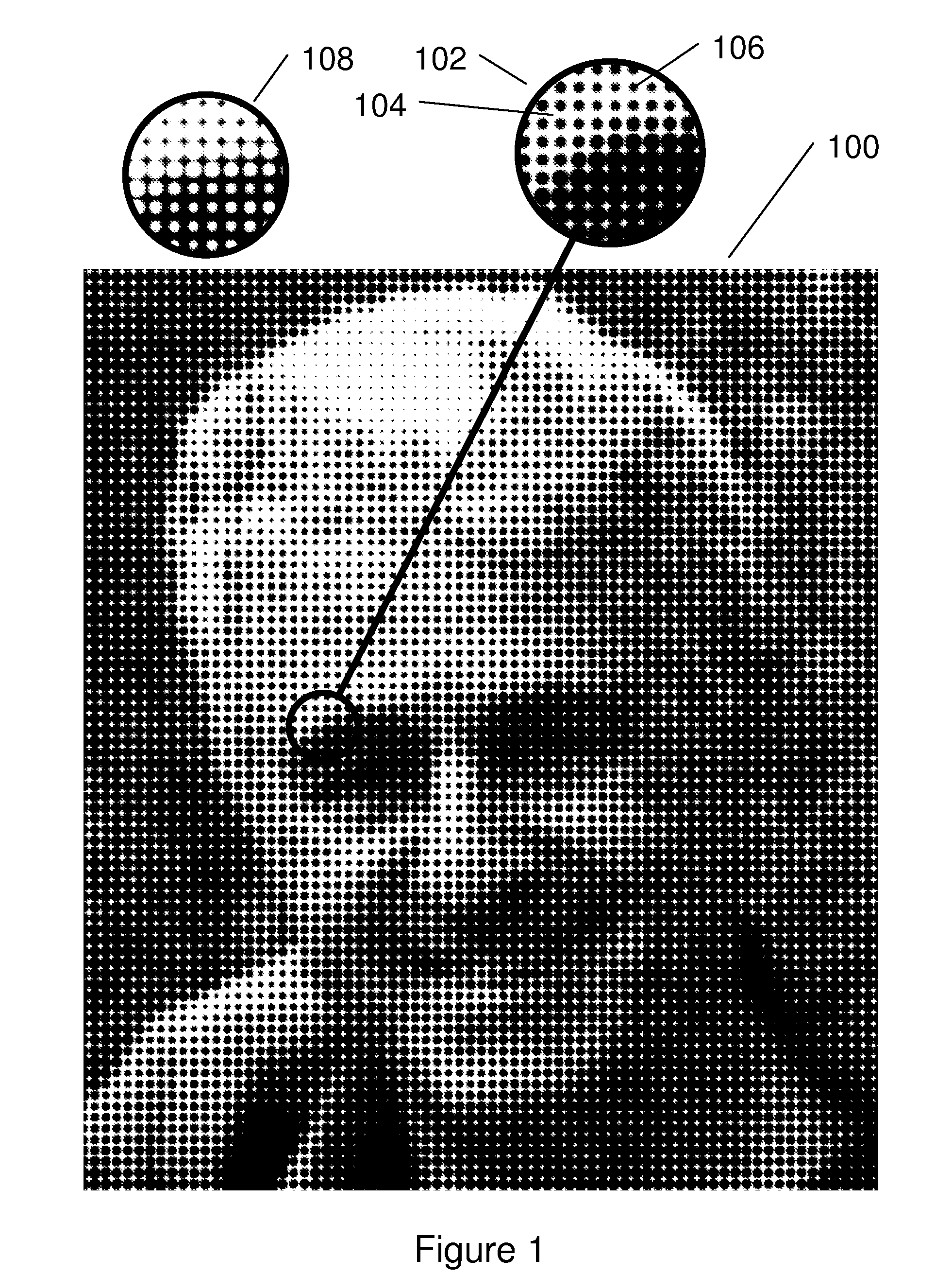
[0022]Reference is made now to FIG. 1, which is a general description of one preferred embodiment of the invention. In this embodiment a portrait 100 of a person is impressed on the chip using aluminum layer over a silicon substrate. 102 is an enlargement of the right eyebrow section, showing details of the modulation of the aluminum layer 104 over the silicon layer 106.

[0023]In this configuration the aluminum layer (represented by the white areas 104) is brighter then the silicon layer (represented by the dark areas 106).

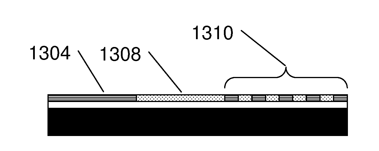
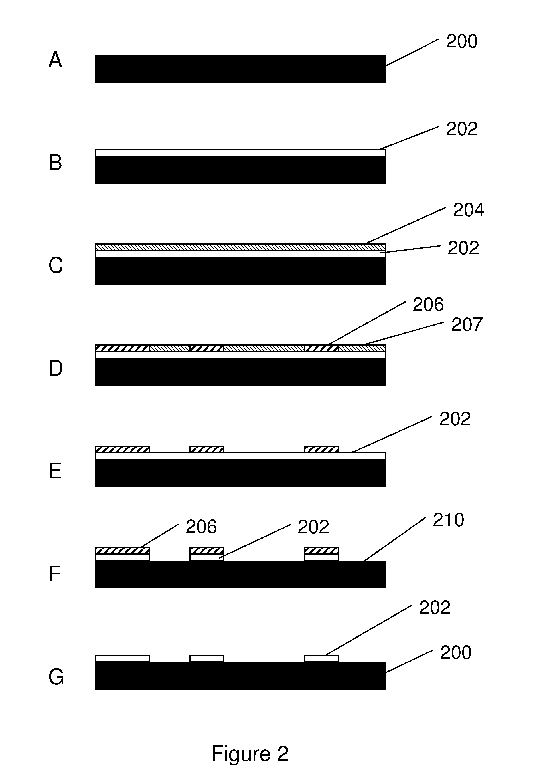
[0024]In an example of 0.6 μm CMOS production technology of semiconductors, the complete height of image 100 is constructed of 1,000 pixels of 0.6 μm resulting in actual physical size of 0.6 mm. The center to center distance between two dark points is 12 pixels, that is 12×0.6 μm=7.2 μm. This design is therefore based on a right-angle grid of rectangles which are 12×12 pixels. Each such 12×12 pixels cell is configured to be partially covered with aluminum and parti...


PUM

PropertyMeasurementUnit
Thicknessaaaaaaaaaa
Angleaaaaaaaaaa
Thicknessaaaaaaaaaa

Abstract

A method and apparatus for producing low cost miniature images is provided. Modulated layers of materials over silicon substrate provide the shades of gray or colors needed to provide the perception of an image. Reflective characteristics as well as refractive characteristics of materials and modulated layers serve to produce the desired effects. Quasi-random geometries eliminate unwanted rainbow impressions. The resultant image is highly resistant to environmental conditions. Metal anodizing and coloring methods as well as metal anodizing interference thin layers methods are used to add more colors to the images. Relatively high-pitch patterns within the image produce secondary visual effects.

Description

FIELD OF THE INVENTION[0001]The invention is related to the field of imaging and more particularly to the field of creating images using microelectronics and other surface treatment technologies.BACKGROUND OF THE INVENTION[0002]Miniature images have been produced for decades using many techniques. Oil painting has been mastered by some artists to create images smaller even then 3 mm×3 mm. These images are hand-made and unsuitable for mass production. Photography is another technique useful for the creation of miniature images. With a typical resolution of 50 points / mm for photographic media, 2 mm×2 mm images can be created using mass production methods, thus reducing the cost per copy. Nevertheless, photographic materials are not durable and need additional production steps to encapsulate them and bring them to a form that is durable in a harsh environment that includes human handling and natural light radiation.[0003]It is the purpose of the present invention to propose apparatus a...

Claims


Application Information

Patent Timeline
IPC IPC(8): G02B5/28B32B3/10
CPCY10T428/24802G02B5/286
Inventor MELMAN, HAIM ZVI
Owner MELMAN HAIM ZVI
Why Eureka
Try Eureka