
Method of manufacturing liquid crystal panel

Inactive Publication Date: 2011-03-10
MITSUBISHI ELECTRIC CORP
View PDF4 Cites 15 Cited by
  • Summary
  • Abstract
  • Description
  • Claims
  • Application Information

AI Technical Summary

Benefits of technology

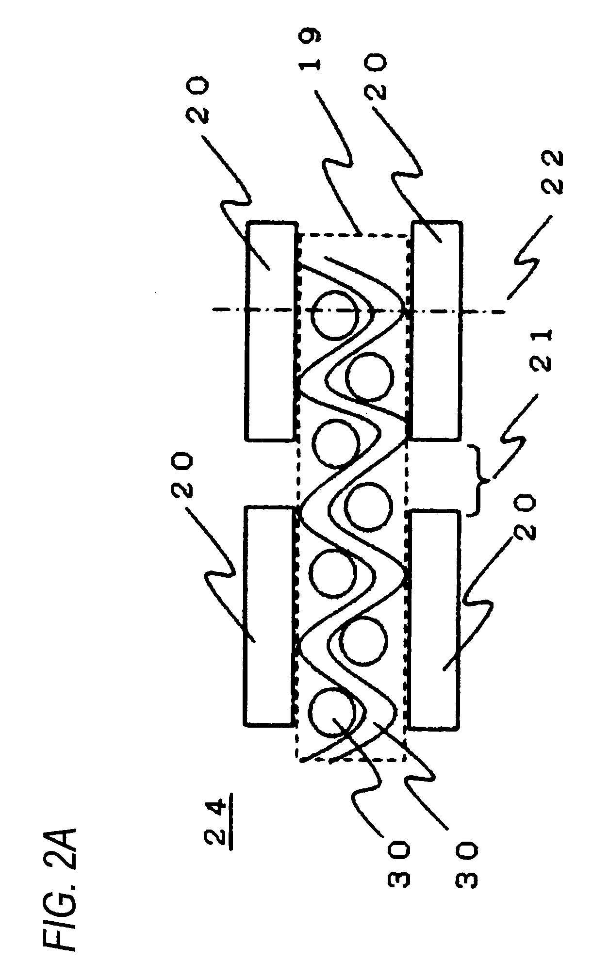
[0016]According to the invention, in the seal printing process, the mesh cross-points of the seal plate are provided to contact with BM regions of a CF substrate and perform the printing. Although the suppression of the mesh marks is not possible, it is possible to take the mesh marks out of the display region (out of a CF opening section) by making the mesh marks in the BM regions of the CF substrate. As a result, a liquid crystal panel having a high image quality can be manufactured without a recognizing the mesh marks. Further, since a uniform pressure can be applied to the seal plate without changing the thickness of the seal plate, the uniformity of the original seal printing width can be kept, and the yield deterioration in the seal printing process can be suppressed.

Problems solved by technology

However, there is a problem that the manufacturing takt-time is lengthened by the applying work without lifting.
Although using a plurality of syringes for shortening the manufacturing takt-time may be considered, the scale of equipment is enlarged and a lot of time is required in preparing the applying work.
However, since the seal plate contact with the display area in the liquid crystal panel, an alignment layer may be damaged.
The damage causes an alignment state of the liquid crystals to be scattered (abnormal alignment area) and to worsen the image quality.
Further, in severe case, the damaged liquid crystal panel becomes defective product and cause to the yield deterioration.
Thus, the alignment layer is damaged, and a large number of abnormal alignment areas (hereinafter referred to as “mesh marks”) 12 occur.
However, even in either of the above-described cases, although an improvement to suppress the occurrence of the mesh marks 12 is accomplished, a uniform pressure is not applied over the entire seal plate during the seal printing process due to the change of the thickness of the seal plate.
Thus, the width of the seal printed section becomes non-uniform (becoming thickened, cracked and the like).
The non-uniformed printed section causes the finished quality of the seal print itself to deteriorate and also cause the yield in the seal printing process to deteriorate.

Method used


Image

  • Method of manufacturing liquid crystal panel
  • Method of manufacturing liquid crystal panel
  • Method of manufacturing liquid crystal panel

Examples


embodiment 1

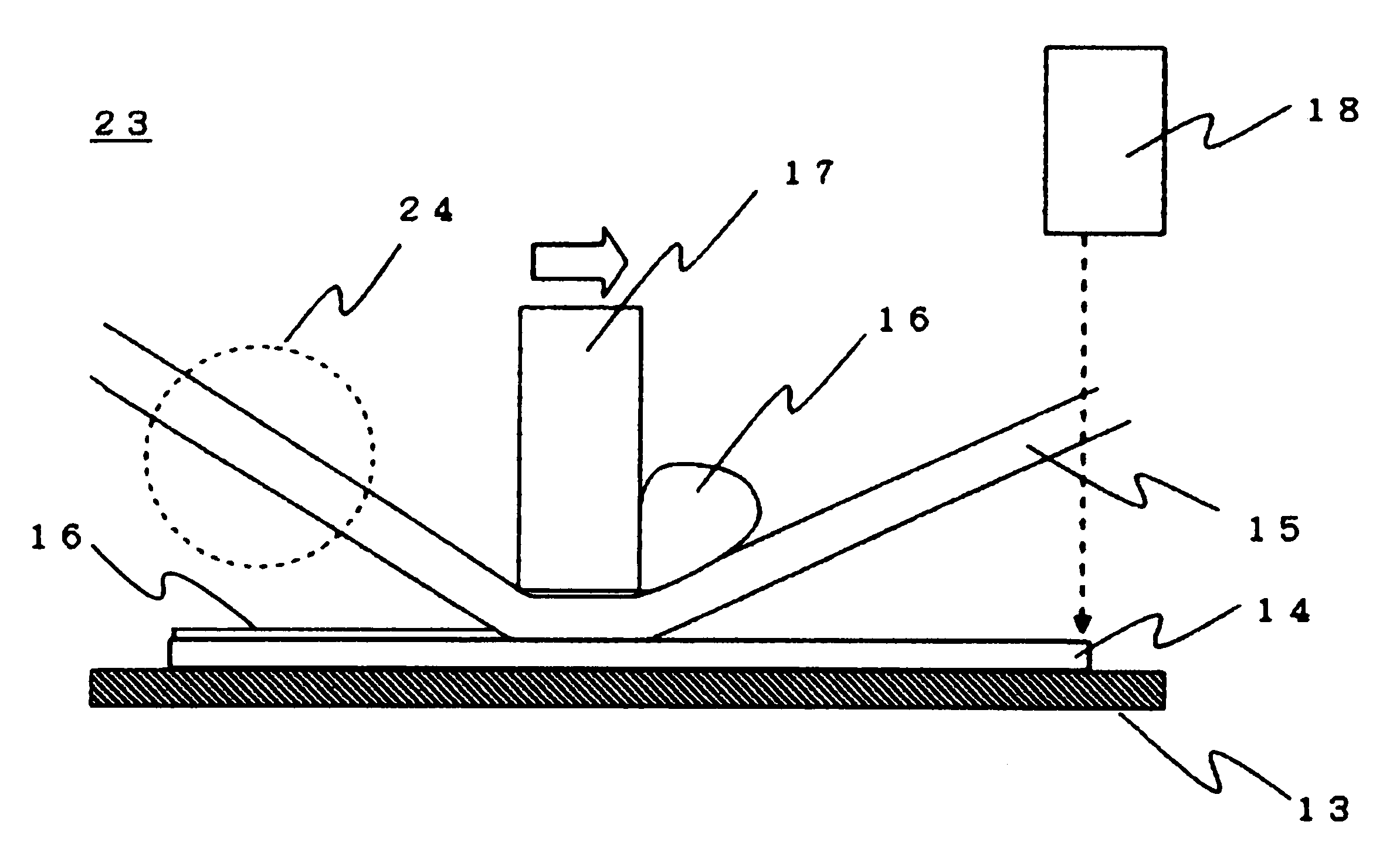
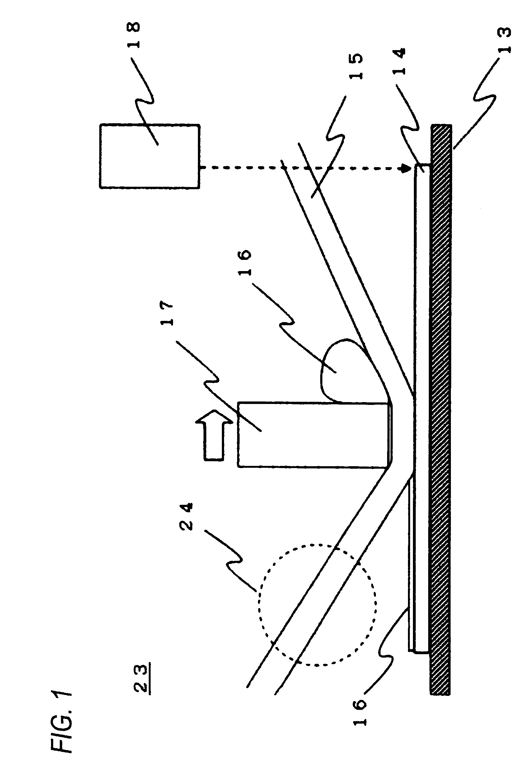
[0024]Hereinafter, embodiment 1 of the invention will be described with reference to the accompanying drawing. First, as shown in FIG. 1, a seal printer 23 is necessary to seal-print of a circumferential seal on a glass substrate by using a seal plate 15. The seal printer 23 includes a seal print stage 13, a seal plate 15, a seal squeegee 17, and an alignment camera 18.

[0025]In order to seal-print a sealant 16 on the glass substrate (in this embodiment, CF substrate 14), the CF substrate 14 where alignment marks (not illustrated) are printed is put on the seal print stage 13, and the camera 18 having an alignment function is provided. A seal printing position is controlled by performing a position control between the seal plate 15 having an outline section where alignment marks (not illustrated) are provided and the CF substrate 14. The sealant 16 is put on the seal plate 15, and then the seal squeegee 17 is pressing and sliding on the seal plate 15 in a direction along with an arro...

embodiment 2

[0033]FIG. 5 is a schematic view showing the occurrence positions of the mesh marks 12 in the case of seal printing using the seal plate according to embodiment 2 of the invention. As shown in FIG. 5, the center of meshes 31 of the vertical and horizontal fibers is disposed in parallel (zero degree) to the arrangement of the CF pixels (CF opening section 10) so that the cross-point sections 22 correspond to the cross-point sections of the BM region 11 of the CF substrate 14. In this case, it is sufficient to set such that the line pitch of the mesh fiber 30 becomes n times (where, n is a positive integer) that is equal to the arrangement pitch of the CF pixels (CF opening section 10). In this embodiment, since the mesh marks are arranged in the cross section of the BM region 11 having a wide area, there is a tolerance to an alignment deviation of up and down direction, right and left direction.

embodiment 3

[0034]In the embodiment 1 and embodiment 2 as described above, the mesh screen plate including the plain weaved stainless wires is used as the seal plate. In this embodiment, a screen plate adopting called as alpha meshes is used. As is well known, the alpha meshes are a flat screen plate formed by precipitation-forming Ni in an additive method (electroforming method).

[0035]Due to the alpha meshes, this screen plate has a superior dimensional stability, and the mesh pitches can be set somewhat freely. Accordingly, even with fine mesh pitches of 250 and 400 mesh / inch, a high dimensional accuracy can be accomplished. In this embodiment of the invention, this screen plate is used as the seal plate of a liquid crystal panel (in which the dot pitch becomes 249 pixels / inch) having a width across corner of 16 inches and a high resolution of QUXGA (3200 (in width)×2400 (in length) pixels). In this embodiment, in the same manner as in the embodiment 2, an advantageous arrangement against the...


PUM


Abstract

A method of manufacturing a liquid crystal panel including two glass substrates, which face each other and are bonded by a circumference seal of a display area, and which hold a liquid crystal therebetween, comprising the steps of: disposing a seal printing plate comprising a mesh cross-points; and applying the circumference seal on either one of the two glass substrates by using the seal printing plate, wherein the mesh cross-points of the seal printing plate contact with a light shielding region of pixels in the display area.

Description

CROSS-REFERENCE TO RELATED APPLICATION[0001]This application claims priority from Japanese Patent Application No. 2009-204718 filed on Sep. 4, 2009, the entire subject matter of which is incorporated herein by reference.BACKGROUND[0002]1. Technical Field[0003]The present invention relates to a method of manufacturing an active matrix type liquid crystal panel that is driven by thin film transistors formed on a glass substrate. Specifically, the present invention relates to a method of manufacturing a liquid crystal panel that is suitable to be applied to a process of printing a sealant on a glass substrate by using a seal plate.[0004]2. Description of the Related Art[0005]Recently, Flat Panel Displays (FPDs), such as liquid crystal displays, have used in many fields including television receivers, computers, and the like due to their light-weight, ultra-thin, and small power-consumption characteristics. According to the diversity of purpose in the market, it is increasing that a dem...

Claims


Application Information

Patent Timeline
IPC IPC(8): G02F1/1339
CPCG02F1/133351G02F1/1339
Inventor MINOWA, KENICHI
Owner MITSUBISHI ELECTRIC CORP
Learn More