Contact probe pin
a technology of contact probe and contact pin, which is applied in the direction of coupling device connection, instruments, transportation and packaging, etc., can solve the problems of deterioration of tin contained in low adhesion to the device under test, and other problems, to achieve the effect of low adhesion and good electrical conductivity
- Summary
- Abstract
- Description
- Claims
- Application Information
AI Technical Summary
Benefits of technology
Problems solved by technology
Method used
Image
Examples
example 1
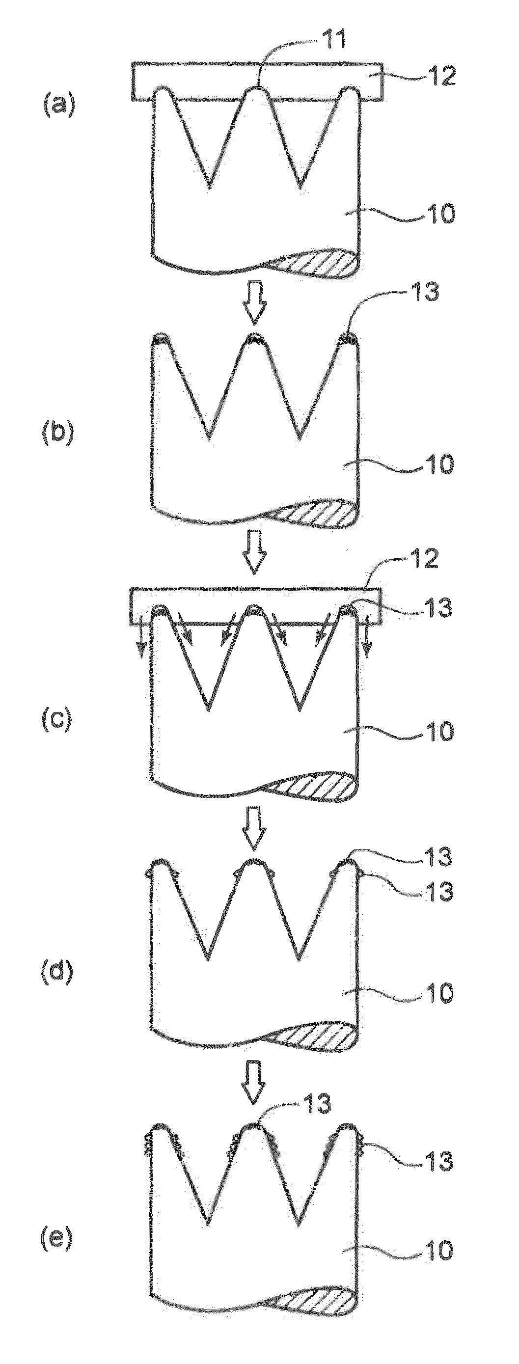
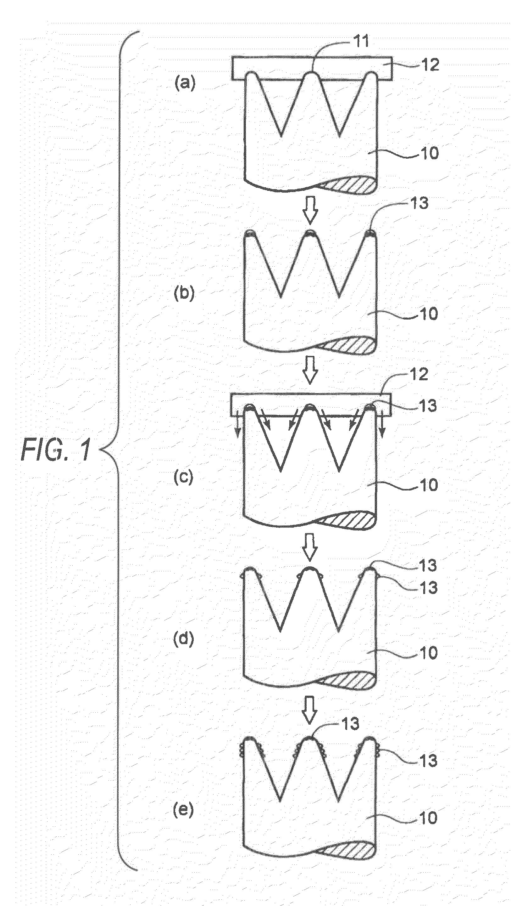
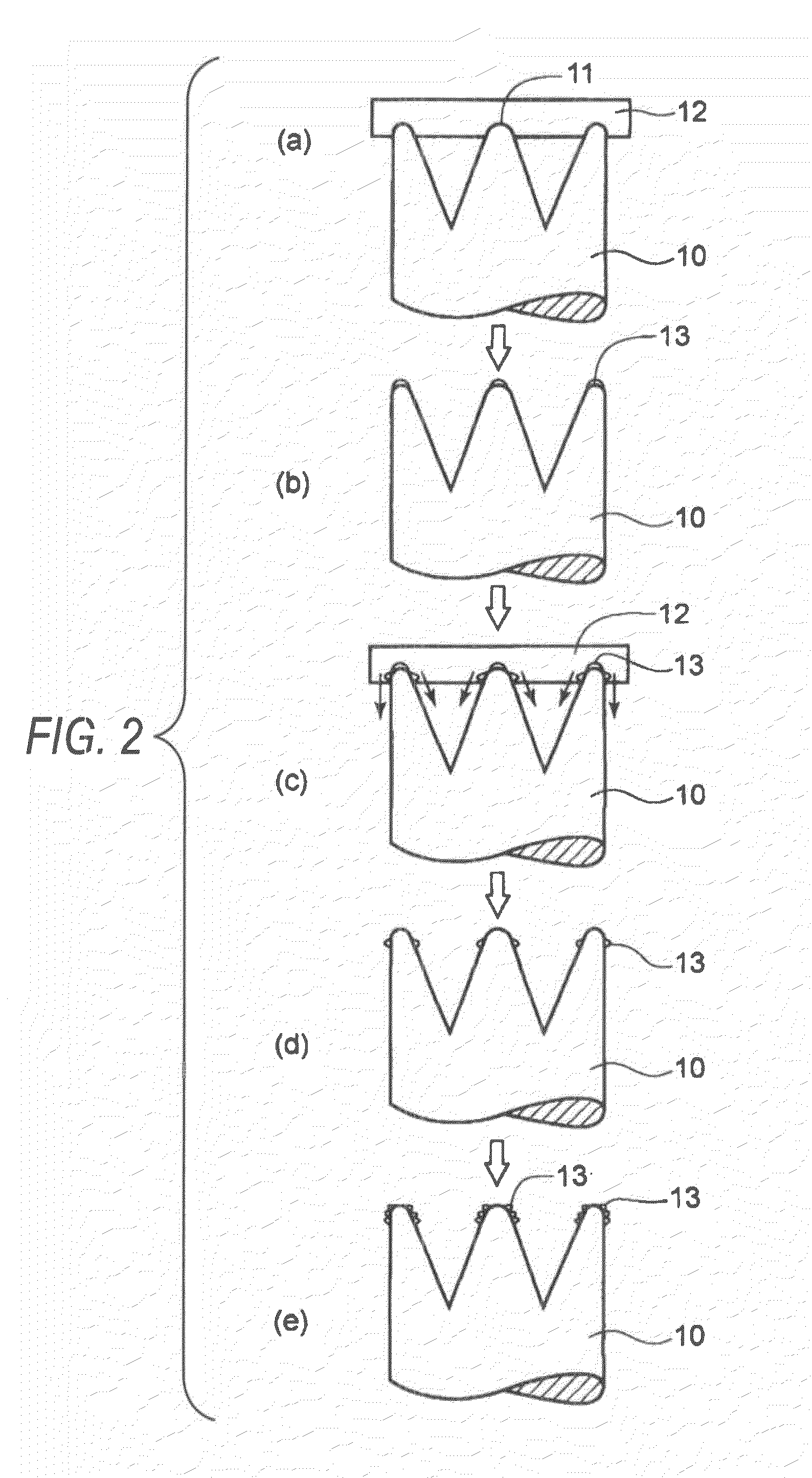
[0048]A spring-containing contact probe pin with the tip part being divided in quarters similarly to those shown in FIGS. 1(a) to 1(e) and FIGS. 2(a) to 2(e) was used. A metal was doped into carbon film, and in order to control the concentration distribution of the metal, the following method was further employed.
[0049]In a parallel plate-type magnetron sputtering apparatus (manufactured by Shimadzu Corporation), a carbon (graphite) target and a chromium target were disposed, and a base material (made of Be—Cu) of the contact probe pin was disposed by arranging its tip part to face the targets (disposed such that the axial core direction of the base material runs perpendicularly to the target face). At this time, for allowing the carbon film to be formed only in a region of about 0.3 mm from the tip part toward the basal part of the contact probe pin, the portion other than that was masked with a jig. Also, the distance between the tip part of the base material and the target was se...
example 2
[0058]A carbon film was formed under the same conditions as in Example 1 except for changing the bias voltage to −100 V and analyzed for the composition (atomic %) at each position in the same manner.
(Results of Composition Analysis)
[0059]Tip part: C: 73.0, Ar: 4.1, W: 22.9
[0060]Lateral part (position at 10 μm, outer peripheral surface): C: 76.1, Ar: 4.1, W: 19.8
[0061]Lateral part (position at 10 μm, inner peripheral surface): C: 78.78, Ar: 3.57, W: 17.65
[0062]Lateral part (position at 20 μm, outer peripheral surface): C: 77.4, Ar: 3.7, W: 18.9
[0063]Using the contact probe pin having formed thereon the carbon film as above (Examples 1 and 2), a contact energization test was performed 100,000 times on an electrode composed of a lead-free solder (Sn+3 atomic % Cu+0.5 atomic % Ag), as a result, it was confirmed that the contact probe pin exhibits excellent resistance stability as compared with the conventional contact probe pin (Au-plated product).
example 3
[0067]The relationship between the content of W in the carbon film and the electric resistance (specific resistance) was examined. At this time, as a specimen, a carbon film (thickness: 0.5 μm) was formed on an insulating substrate by variously changing the content of W (the content was measured by EPMA), and the specific resistance of each carbon film was measured by the following method.
(Method for Measuring Specific Resistance)
[0068]The sheet resistance of the thin film was measured using a commercially available measuring instrument (3226 mΩ HI TESTER manufactured by Hioki E. E. Corporation+a four-probe measuring device manufactured by Kyowa Riken Ltd.) according to a four probe method generally employed in the measurement of resistance of a thin film, and the specific resistance was calculated by multiplying the measured value by the film thickness and a correction factor for sheet resistance (=4.532).
[0069]The results (the relationship between the content of W and the specific...
PUM
| Property | Measurement | Unit |
|---|---|---|
| contact resistance | aaaaa | aaaaa |
| thickness | aaaaa | aaaaa |
| thickness | aaaaa | aaaaa |
Abstract
Description
Claims
Application Information
 - R&D
- Intellectual Property
- Life Sciences
- Materials
- Tech Scout
- Unparalleled Data Quality
- Higher Quality Content
- 60% Fewer Hallucinations
Browse by: Latest US Patents, China's latest patents, Technical Efficacy Thesaurus, Application Domain, Technology Topic, Popular Technical Reports.
© 2025 PatSnap. All rights reserved.Legal|Privacy policy|Modern Slavery Act Transparency Statement|Sitemap|About US| Contact US: help@patsnap.com


