A/d converter unit for image sensor

Inactive Publication Date: 2011-02-03
CURIOUS CORP
View PDF10 Cites 23 Cited by
  • Summary
  • Abstract
  • Description
  • Claims
  • Application Information

AI Technical Summary

Benefits of technology

[0021]Accordingly, in consideration of such an actual situation, it is an object of the present invention to provide an A / D converter unit using a column A / D converter of a reduced size, enabling high-speed readout as well as high resolution.
[0023]According to the present invention, it is possible to obtain an A / D converter unit using a high-resolution, high-speed column A / D converter with a reduced size. Further, even in a high-definition image sensor having a large number of pixels with a narrow pitch of pixel arrangement, it is possible to obtain a function of being capable of outputting high-quality digital image signals at a high frame rate.

Problems solved by technology

This makes it difficult to reduce current consumption.
However, even when using the APS CMOS image sensor (hereafter expressed as CMOS image sensor or simply, image sensor), the situation is that, to achieve high speed with maintained high resolution, the increase of current consumption in an A / D converter to convert analog signals into digital signals is inevitable.
This causes deteriorated performance of A / D conversion, and it is not possible to reduce the capacitor area accordingly.
Thus, the method has a defect that realization of high resolution is difficult in a column A / D converter requiring a narrow pitch formation.
This produces a serious demerit of difficulty in obtaining high resolution.
However, it is becoming difficult in recent years to arrange such highly accurate operational amplifiers into columns with a slender-shaped layout to fit to a narrow pixel pitch.
Such a fine transistor has a low voltage tolerance that requires a low power supply voltage, and therefore, it is not possible to ensure enough dynamic range of the operational amplifier.
From the viewpoint of high speed, the single slope method is extremely difficult.
On the other hand, to obtain a multi-bit A / D converter unit using the aforementioned simple charge-redistribution successive approximation A / D converters, an extremely large number of elements are required, which is unsuitable for a column A / D converter having a large restriction in size.
However, if it is intended to apply the above-mentioned method intact to a column A / D converter, there are problems described below.
One is that, if it is intended to include the resistor string in each column A / D converter, the resistor area is too large to fit in a narrow pitch.
Therefore, if variation exists in each unit resistor forming the resistor string, the variation leads to the deterioration of a nonlinearity error.
This causes a drawback that the overall circuit area becomes large.
However, it is not suitable for a column A / D converter having a strict restriction of size.

Method used


Image

  • A/d converter unit for image sensor
  • A/d converter unit for image sensor
  • A/d converter unit for image sensor

Examples


embodiment 1

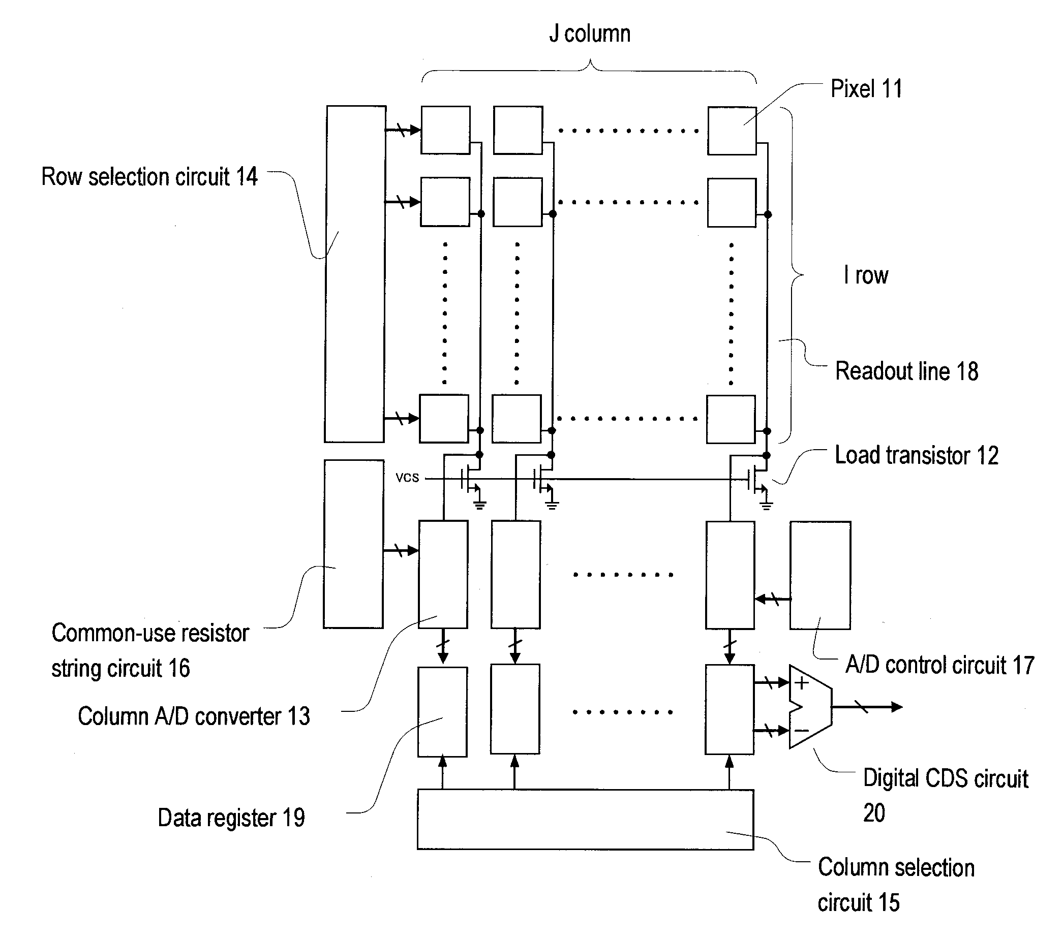
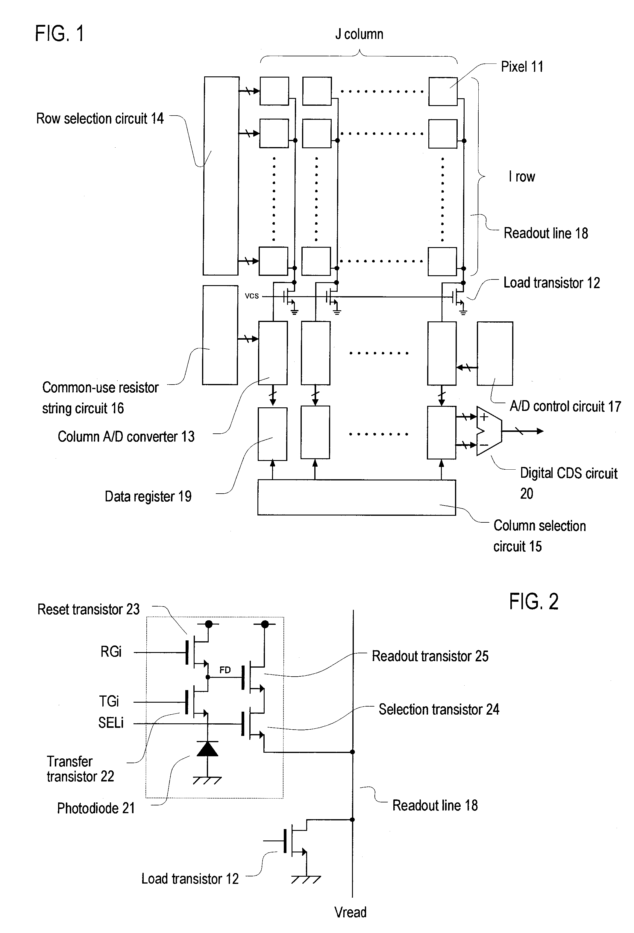
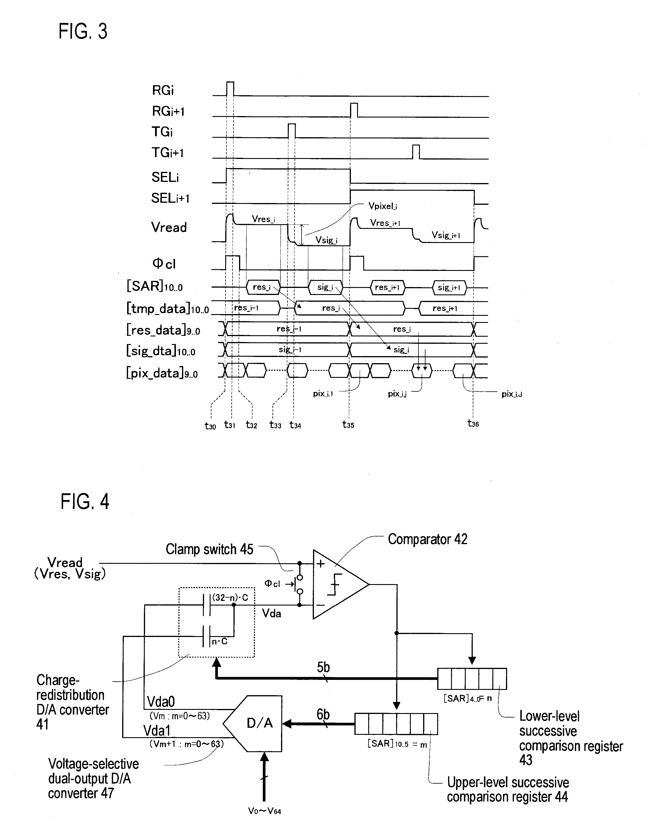
[0038]FIGS. 1 through 12 show an embodiment of the invention, in which like symbols designate like parts. FIG. 1 is a block diagram illustrating an overall configuration of an image sensor according to the present embodiment. A pixel (11) to which photoelectric conversion is to be performed is arranged in a two-dimensional matrix of I rows and J columns. Each pixel in a row selected by a row selection circuit (14) is connected to a readout line (18) of each column. By that a bias current is supplied by a load transistor (12), a signal of the selected pixel is output from a sensor signal output terminal (Vread). In an APS CMOS image sensor, to avoid an influence caused by a pixel-by-pixel difference of readout transistor threshold voltages and a reset noise represented by a kTC noise etc., a signal charge amount stored in a photodiode has to be obtained with accuracy. For this purpose, a method called CDS (Correlated Double Sampling) is generally used, by which a difference is obtain...


PUM


Abstract

A high-speed, high-resolution column A / D converter having a noise reduction function to eliminate a fixed pattern noise etc. is provided with a small circuit scale. Each column A / D converter includes a dual-output D / A converter for selecting two reference voltages from among a reference voltage group supplied in common to each column A / D converter, so as to output the two reference voltages to sandwich each sensor signal voltage input to each column A / D converter, along with a charge-redistribution D / A converter having a full scale determined by the above two reference voltages. Thus, the high-speed, high-resolution column A / D converter is achieved with a small circuit scale. Further, by the utilization of high-speed conversion capability, noise reduction is performed through digital calculation after the A / D conversion.

Description

CROSS-REFERENCE TO RELATED APPLICATIONS[0001]This application is based upon and claims the benefit of priority from the prior Japanese Patent Application No. 2009-180542, filed on Aug. 3, 2009, the entire contents of which are incorporated herein by reference.BACKGROUND OF THE INVENTION[0002]1. Field of the Invention[0003]The present invention relates to an A / D converter unit for an image sensor for converting the output of an analog image from the image sensor into digital data and in particular, an A / D converter unit appropriate for an image sensor having column arrangement.[0004]2. Background of the Related Art[0005]In a digital still camera and a mobile phone camera, conventionally, CCD and APS (active pixel sensor) CMOS image sensors have been in use. In accompany of higher resolution in recent years, the number of pixels tends to be increased. Meanwhile, there are also requirements for high speed continuous shooting, high frame-rate moving images, etc. In combination of the ab...

Claims


Application Information

Patent Timeline
IPC IPC(8): H04N5/335H03M1/34
CPCH03M1/14H04N5/378H03M1/804H03M1/68H04N25/78H04N25/75
Inventor HASEGAWA, JUN
Owner CURIOUS CORP
Why Eureka
Try Eureka