Reference voltage generation circuit, a/d converter and d/a converter

a reference voltage generation and converter technology, applied in the direction of digital-analog converters, power saving provisions, instruments, etc., can solve the problems of suppressing power consumption and large power reduction, and achieve the effect of reducing power consumption and reducing flow curren

Inactive Publication Date: 2010-11-18
PANASONIC CORP
View PDF6 Cites 6 Cited by
  • Summary
  • Abstract
  • Description
  • Claims
  • Application Information

AI Technical Summary

Benefits of technology

[0020]An object of the present invention is to provide a reference voltage generation circuit in which a transition time to a power-saving mode and a recovery time are short and an intermittent operation in a short period of time can be performed. Another object of the present invention is to provide an A / D converter and a D / A converter using the reference voltage generation circuit.
[0022]In the reference voltage generation circuit with this configuration, a flowing current can be reduced by raising the resistance between the first reference voltage terminal and the second reference voltage terminal during the power-saving mode. Further, the voltage of the capacitor for storing charge between the first reference voltage terminal and the second reference voltage terminal is held by the current control circuit. Therefore, a recovery time from the power-saving mode is short, an intermittent operation in a short period of time can be performed, and the power-saving mode for reducing power consumption can be used frequently.

Problems solved by technology

These methods lead to the large reduction in power when the A / D converter or the D / A converter is applied to equipment that is not in continuous use at all times.
Thus, there is a problem that, only when the time for activation can be ensured sufficiently, is the suppression of power consumption allowable.

Method used


Image

  • Reference voltage generation circuit, a/d converter and d/a converter
  • Reference voltage generation circuit, a/d converter and d/a converter
  • Reference voltage generation circuit, a/d converter and d/a converter

Examples


embodiment 1

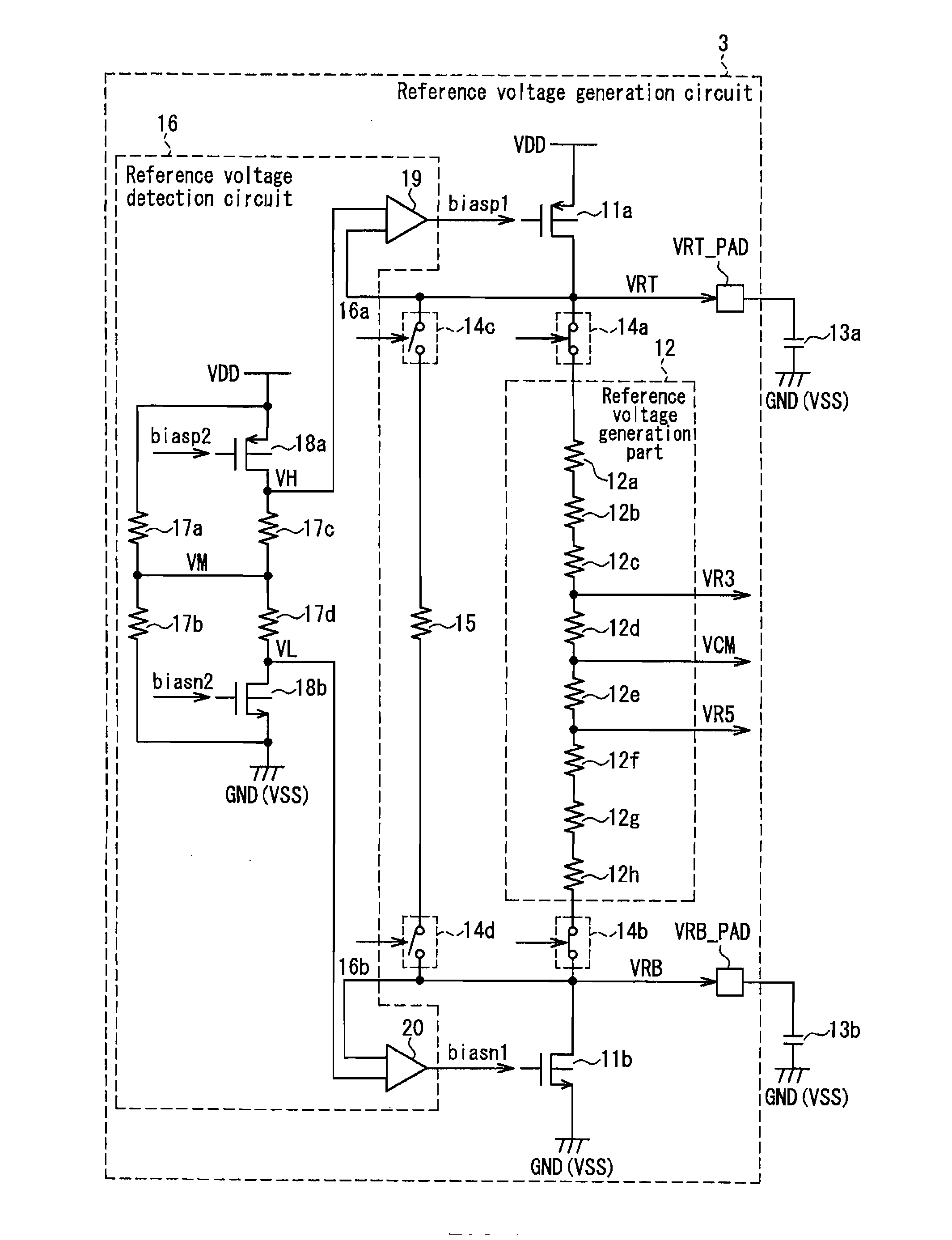
[0037]FIG. 1 is a circuit diagram showing a reference voltage generation circuit in Embodiment 1 of the present invention. The case where this circuit is used as a reference voltage generation circuit for a pipeline type ADC will be exemplified. The same elements as those in the circuit in the conventional example shown in FIG. 6 are denoted with the same reference numerals as those therein.

[0038]The reference voltage generation circuit includes a reference voltage generation part 12 and current bias sources 11a and 11b that allow a constant current to flow. Thus, a circuit similar to the reference voltage generation circuit shown in FIG. 6 is configured. Further, as the feature of the present embodiment, a reference voltage detection circuit 16 for controlling the current bias sources 11a and 11b is provided.

[0039]The reference voltage generation part 12 includes eight voltage-dividing resistors 12a to 12h having an equal resistance value. The current bias source 11a has a P-channe...

embodiment 2

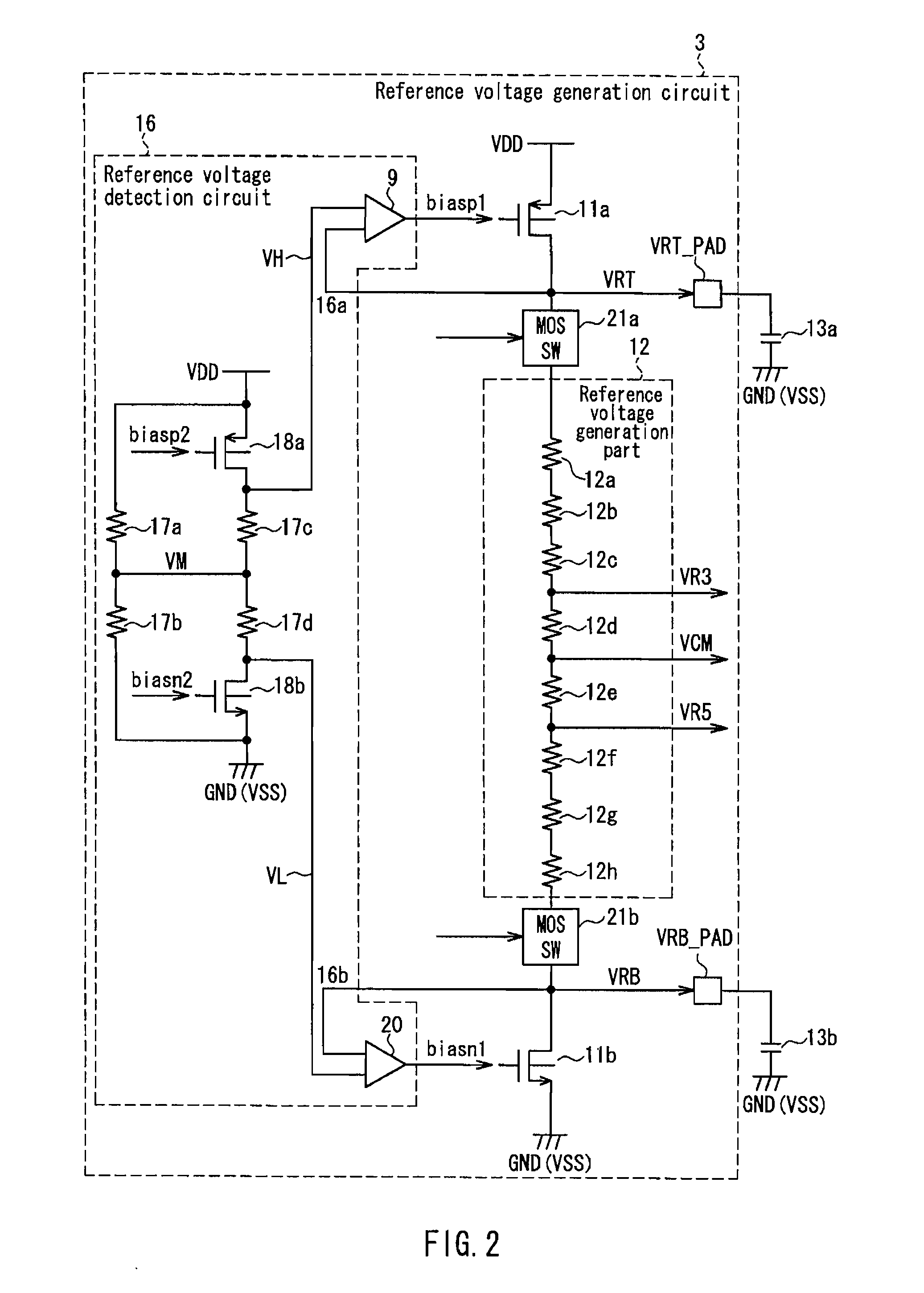
[0052]FIG. 2 is a circuit diagram showing a reference voltage generation circuit in Embodiment 2 of the present invention. In this circuit, the same elements as those in the circuit of Embodiment 1 shown in FIG. 1 are denoted with the same reference numerals as those therein.

[0053]In the reference voltage generation circuit of the present embodiment, a MOS SW 21a is connected between the reference voltage terminal VRT and the voltage-dividing resistor 12a and a MOS SW 21b is connected between the reference voltage terminal VRB and the voltage-dividing resistor 12h in place of the analog SWs 14a to 14d and the high resistance resistor 15 in Embodiment 1. The MOS SWs 21a, 21b are in an ON state during a normal mode, and supply a current to the voltage-dividing resistors 12a to 12h at a low resistance value.

[0054]The MOS SW is capable of changing a resistance value by controlling a gate voltage. Therefore, during a power-saving mode, the resistance values of the MOS SWs 21a, 21b can be...


PUM


Abstract

A reference voltage generation circuit of the present invention includes: a reference voltage generation part 12 that is connected between a first reference voltage terminal VRT and a second reference voltage terminal VRB and that generates a plurality of reference voltages when being supplied with a power supply current from the first and second reference voltage terminals; capacitors 13a, 13b for storing charge that are connected to the first and second reference voltage terminals, respectively; a reference voltage detection circuit 16 that detects voltage values at the first and second reference voltage terminals; current control circuits 11a, 11b that control a magnitude of a power supply current that is allowed to flow through the reference voltage generation part so that the first and second reference voltage terminals are kept at predetermined voltage values, in accordance with the voltage values detected by the reference voltage detection circuit; and switching parts 14a to 14d that switch the connection between the first and second reference voltage terminals so as to replace the reference voltage generation part with a high-resistance element 15. During a power-saving mode, the reference voltage generation part is switched to the high-resistance element, whereby a current flowing between the first and second reference voltage terminals is reduced, and the potentials of the capacitors are kept due to a minute current. Therefore, a recovery time from the power-saving mode becomes short.

Description

BACKGROUND OF THE INVENTION[0001]1. Field of the Invention[0002]The present invention relates to a reference voltage generation circuit that generates a plurality of reference voltages by resistance voltage division from two reference voltages generated with a power supply current. The present invention also relates to an A / D converter that generates a digital signal by quantizing an input analog signal based on a plurality of reference voltages, and a D / A converter that generates an analog signal from an input digital signal.[0003]2. Description of Related Art[0004]As digitization proceeds in an AV field, an information communication field, and the like, there is an increasing demand for high speed and high precision in an A / D converter and a D / A converter that are key devices, and at the same time, there also is a demand for lower power consumption that contradicts the performance.[0005]Examples of the A / D converter widely used in the AV field, the information communication field,...

Claims


Application Information

Patent Timeline
Patent Type & Authority Applications(United States)
IPC IPC(8): H03M1/66G05F3/16H03M1/34
CPCH03M1/002H03M1/0695H03M1/765H03M1/44H03M1/365
Inventor KITO, TAKAYASU
Owner PANASONIC CORP
Why Eureka
Try Eureka