
Group iii nitride semiconductor device and light-emitting device using the same

a technology of nitride and semiconductors, applied in the direction of semiconductor devices, basic electric elements, electrical appliances, etc., can solve the problems of large amount of crystal defects, high dissociation pressure, and failure to retain single crystals, etc., to achieve high reverse withstand voltage and improve crystallinity

Inactive Publication Date: 2010-10-21
RESONAC HOLDINGS CORPORATION
View PDF6 Cites 4 Cited by
  • Summary
  • Abstract
  • Description
  • Claims
  • Application Information

AI Technical Summary

Benefits of technology

The solution results in a Group III nitride semiconductor device with improved crystallinity and high reverse withstand voltage, enhancing the performance and reliability of light-emitting devices by optimizing the substrate layer structure and growth process.

Problems solved by technology

Growing only a nitride single crystal itself has been considered difficult, for the following reasons.
Nitrogen, which is a constituent of the single crystal, has high dissociation pressure and therefore fails to be retained in the single crystal in, for example, the pulling method.
However, even when a nitride semiconductor single crystal is grown directly on such a single-crystal substrate, large amounts of crystal defects, which are attributed to crystal lattice mismatch between the crystalline substrate and the single crystal, are generated in the resultant nitride semiconductor single crystal film; i.e., the epitaxial film fails to exhibit good crystallinity.

Method used


Image

  • Group iii nitride semiconductor device and light-emitting device using the same
  • Group iii nitride semiconductor device and light-emitting device using the same
  • Group iii nitride semiconductor device and light-emitting device using the same

Examples


example

[0045]FIG. 5 is a schematic representation showing the Group III nitride semiconductor light-emitting device of the present invention produced in the present Example. Reference numeral 1 denotes a substrate composed of sapphire. Semiconductor layers were grown along the crystal plane orientation of the substrate. A first layer 2 composed of Al0.08Ga0.92N doped with Si (5×10¹⁸ atoms / cm3) was formed on the substrate. A second layer 3 composed of an undoped GaN single crystal layer, and an n-type GaN single crystal layer 4 doped with Si (1×10¹⁸ atoms / cm3) were successively formed on the first layer 2. A light-emitting layer 6 was formed, via a Ga0.98In0.02N layer 5, on the Si-doped GaN single crystal layer 4. The Ga0.98In0.02N layer 5 is provided between the Si-doped GaN layer 4 and the light-emitting layer 6 for preventing propagation of crystal defects from the Si-doped GaN layer 4.

[0046]The light-emitting layer 6 has a structure including a plurality of stacked layer units, each inc...


PUM

PropertyMeasurementUnit
heightaaaaaaaaaa
widthaaaaaaaaaa
sizeaaaaaaaaaa

Abstract

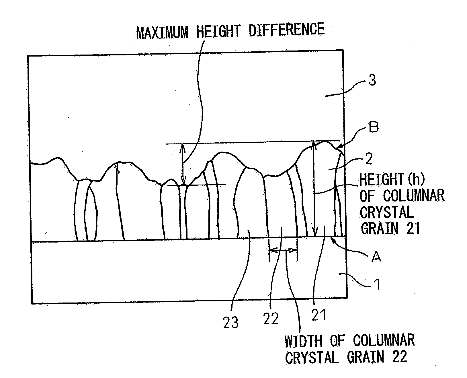
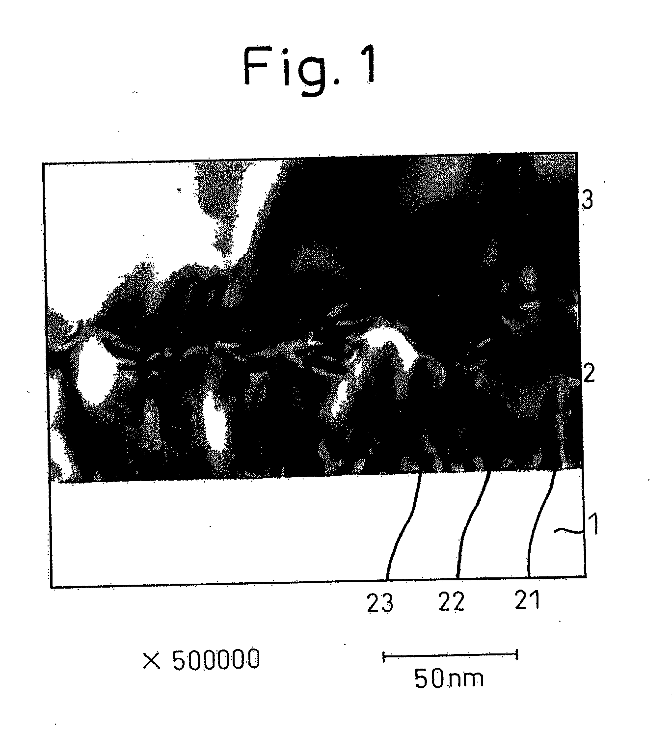
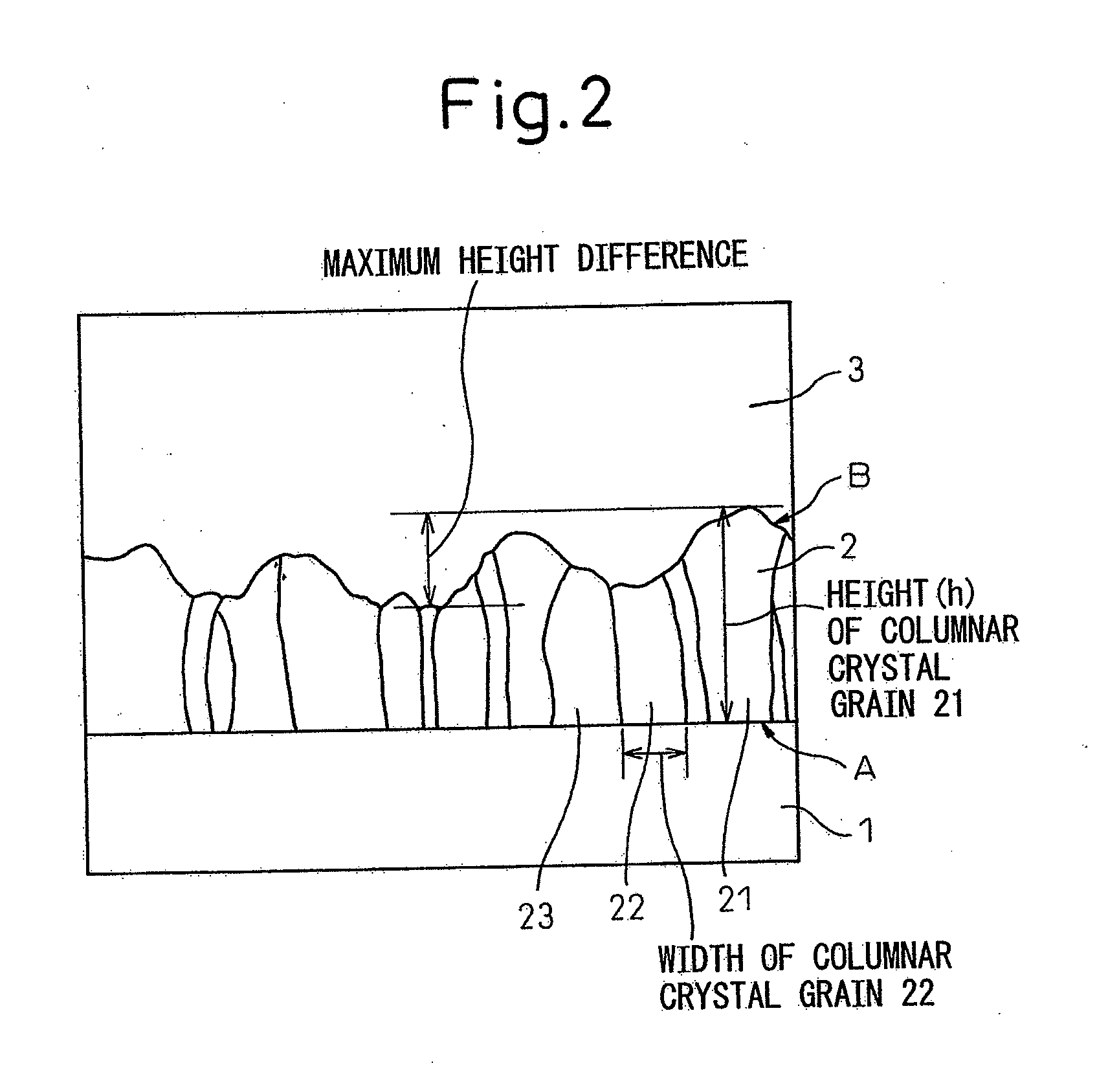
A Group III nitride semiconductor device and method for producing the same. The device includes a substrate, and a plurality of Group III nitride semiconductor layers provided on the substrate. A first layer which is in contact with the substrate is composed of AlxGa1-x N (0≦x≦1), and the difference in height between a protrusion and a depression which are present at the interface between the first layer and a second layer provided thereon is 10 nm or more and is equal to, or less than, 99% the thickness of the first layer. The method includes a first step of depositing on a substrate, a layer containing fine Group III metal particles containing silicon; a second step of nitridizing the fine particles in an atmosphere containing a nitrogen source; and a third step of growing a Group III nitride semiconductor single crystal on the thus-nitridized fine particles.

Description

CROSS REFERENCE TO RELATED APPLICATION[0001]This application is a Divisional of U.S. application Ser. No. 10 / 583,336 filed on Jun. 19, 2006, which further claims priority from U.S. Provisional Application No. 60 / 532,924 filed on Dec. 30, 2003, the entire disclosures of which are incorporated herein by reference.TECHNICAL FIELD[0002]The present invention relates to a Group III nitride semiconductor device, exhibiting good crystallinity, which is employed in, for example, light-emitting diodes, laser diodes, and electronic devices.BACKGROUND ART[0003]Group III nitride semiconductors have a direct transition band structure and exhibit bandgap energies corresponding to the energy of visible to ultraviolet light. By virtue of these characteristics, Group III nitride semiconductors are employed at present for producing light-emitting devices, including blue LEDs, blue-green LEDs, ultraviolet LEDs, and white LEDs (which contain a fluorescent substance in combination with such a nitride sem...

Claims


Application Information

Patent Timeline
Patent Type & Authority Applications(United States)
IPC IPC(8): H01L21/20H01L21/205H01L33/00H01L33/12H01L33/32
CPCH01L21/0237H01L21/0242H01L21/02433H01L21/02458H01L21/02494H01L21/02513H01L33/325H01L21/02576H01L21/02579H01L21/02614H01L21/0262H01L33/007H01L33/12H01L21/0254
Inventor SAKURAI, TETSUO
Owner RESONAC HOLDINGS CORPORATION
Learn More