
Touch sensitive device

a technology of touch sensitive devices and insulating pads, applied in the field of touch sensitive devices, can solve the problems of low capacitance sensitivity, hindering applicability, and inflexible fabricated glass substrates, and achieve the effects of improving waterproofing, optical, planarization or anti-interference performan

Active Publication Date: 2010-10-21
HANNSTAR DISPLAY CORPORATION
View PDF12 Cites 61 Cited by
  • Summary
  • Abstract
  • Description
  • Claims
  • Application Information

AI Technical Summary

Benefits of technology

[0009]In one embodiment, the present invention provides a touch sensitive device. The touch sensitive device includes: a non-conductor soft or hard substrate, or a soft or hard compound substrate comprising gas-water-proof material, anti-reflection optical material, electrode-adhesion-enhanced material, planarization material, or scrape-proof material; a plurality of first electrodes formed on the substrate and arranged along a first direction without overlapping one another; a first insulating layer formed on the substrate and covering the plurality of first electrodes; and a plurality of second electrodes formed on the first insulating layer and arranged along a second direction without overlapping one another, wherein the fist direction is orthogonal to the second direction. An isolating layer is formed on the second electrodes to improve waterproofing, optical, planarization or anti-interference performance.
[0010]In another embodiment, the present invention provides a touch sensitive device. The touch sensitive device includes: a non-conductor soft or hard substrate, or a soft or hard compound substrate comprising gas-water-proof material, anti-reflection optical material, electrode-adhesion-enhanced material, planarization material, or scrape-proof material; a plurality of first electrodes and a plurality of second electrodes formed on the substrate and arranged along a first direction and a second direction without overlapping one another; a first insulating layer formed on the substrate and covering the plurality of first electrodes and second electrodes, and a plurality of cavities are formed on the first insulating layer; a wire layer comprising a plurality of wires formed on the first insulating layer, and the first electrodes are connected by the plurality of wires, wherein the first direction is orthogonal to the second direction. An isolating layer is formed on the wire layer to improve waterproofing, optical, planarization or anti-interference performance.
[0011]In another embodiment, the present invention provides a touch sensitive device. The touch sensitive device includes: a soft or hard substrate, or a soft or hard compound substrate comprising gas-water-proof material, anti-reflection optical material, electrode-adhesion-enhanced material, planarization material, or scrape-proof material; a plurality of first electrodes formed on the substrate and arranged along a first direction without overlapping one another; and a first insulating layer formed on the substrate and covering the plurality of first electrodes; a plurality of second electrodes formed on the first insulating layer and arranged along a second direction without overlapping one another; a preventing layer formed on the first insulating layer and covering the second electrodes, wherein the fist direction is orthogonal to the second direction. An isolating layer is formed under the isolating layer to improve waterproof, optical, planarization or anti-interference performance.
[0012]In another embodiment, the present invention provides a structure of a touch sensitive device. The touch sensitive device includes: a soft or hard substrate, or a soft or hard compound substrate comprising gas-water-proof material, anti-reflection optical material, electrode-adhesion-enhanced material, planarization material, or scrape-proof material; a wire layer comprising a plurality of wires formed on the substrate; a first insulating layer formed on the wire layer and a plurality of cavities are formed in the first insulating layer; a plurality of first electrodes and a plurality of second electrodes formed on the substrate and arranged along a first direction and a second direction without overlapping one another, and the first electrodes are connected by the plurality of wires via the plurality of cavities; and a preventing layer formed on the first insulating layer and covering the plurality of first electrodes and the second electrodes, wherein the first direction is orthogonal to the second direction. An isolating layer is formed between the wire layer and the substrate to improve waterproofing, optical, planarization or anti-interference performance.

Problems solved by technology

While the glass substrate is formed at higher temperatures, beneficial for forming low resistance ITO electrode for fabrication of a stacked structure and large area manufacturing, the fabricated glass substrate is not flexible and has low capacitance sensitivity due to the thickness of the glass substrate, hindering applicability.
Meanwhile, the PET / ITO substrate is formed at lower temperatures, forming high resistance ITO electrodes, hindering fabrication of a stacked structure and large area manufacturing.

Method used


Image

  • Touch sensitive device
  • Touch sensitive device
  • Touch sensitive device

Examples


Embodiment Construction

[0044]In the following detailed description, for purposes of explanation, numerous specific details are set forth in order to provide a thorough understanding of the disclosed embodiments. It will be apparent, however, that one or more embodiments may be practiced without these specific details. In other instances, well-known structures and devices are schematically shown in order to simplify the drawing.

[0045]FIG. 2 is a diagram showing a display device which includes a substrate device 210, a display medium 220 and a bottom device 230. Generally, a touch sensing panel (not showed) is externally bonded to the substrate device 210 and executed by conductors or fingers.

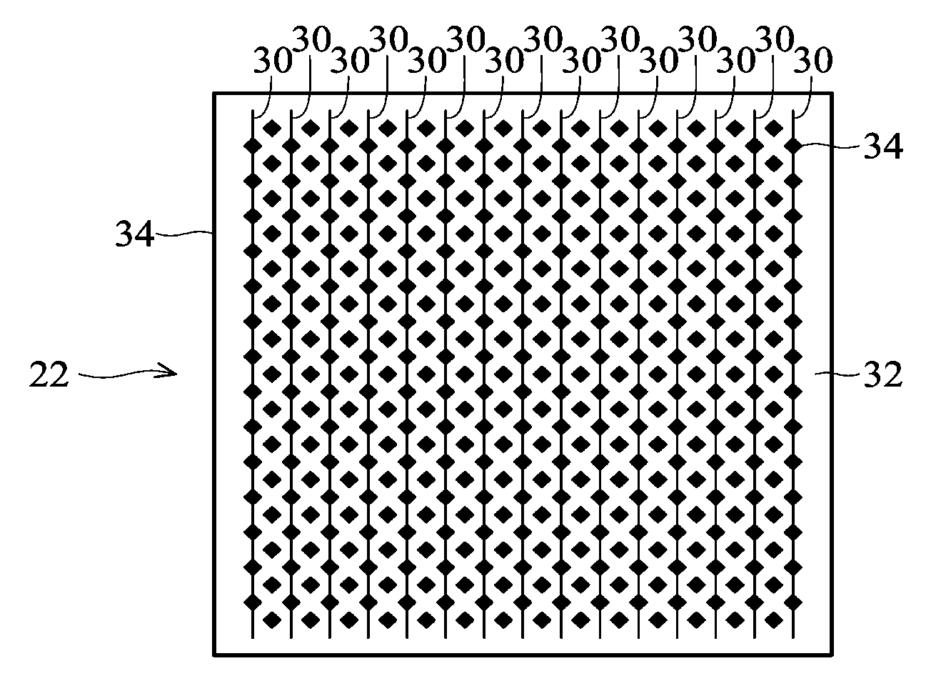
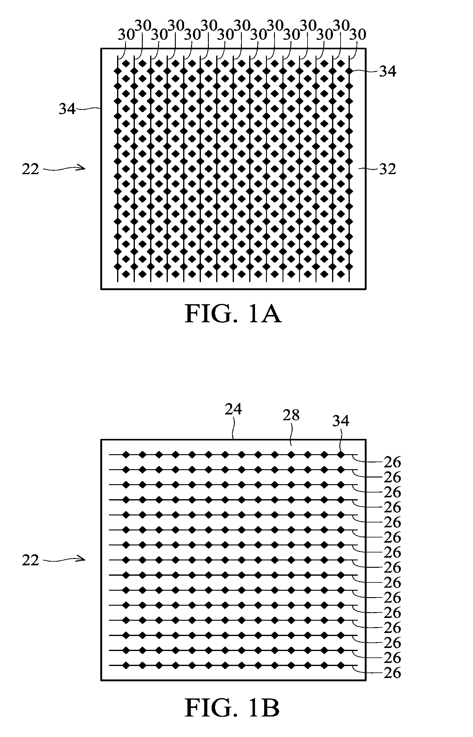
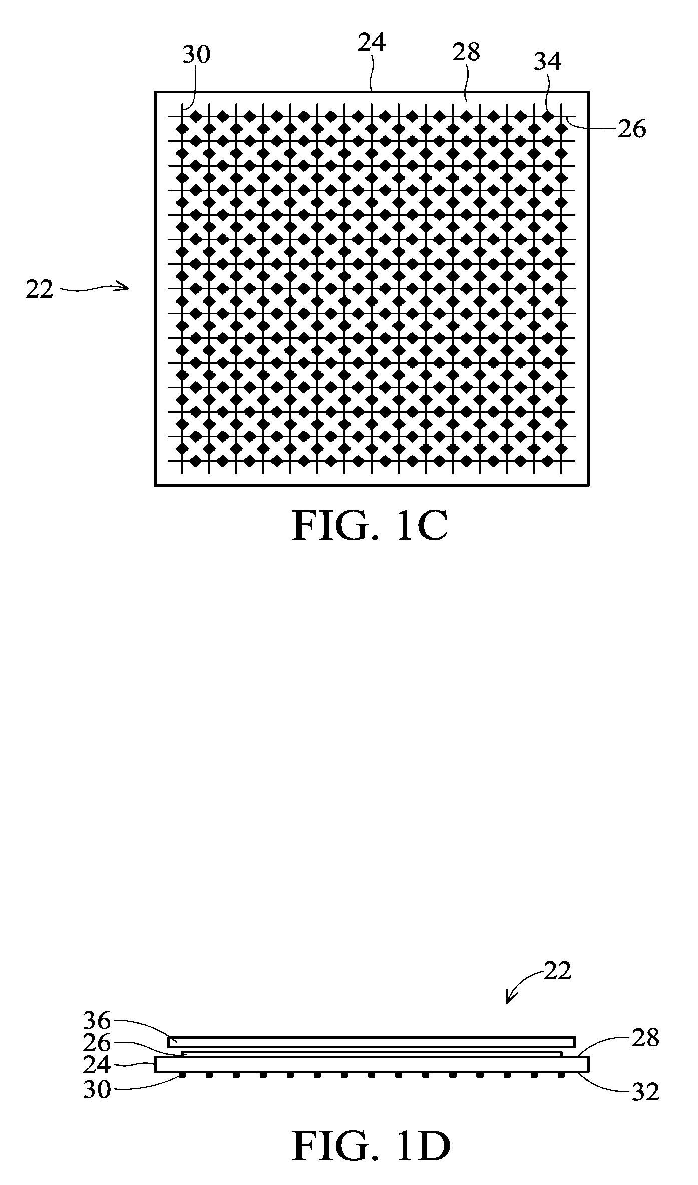
[0046]FIG. 3 is a diagram showing a touch sensitive device of an embodiment of the invention. The touch sensitive device 310 includes a substrate 311, a plurality of first electrodes 312, a first insulating layer 313 and a plurality of second electrodes 314.

[0047]The touch sensitive device 310 includes the substrate 31...


PUM


Abstract

A touch sensitive device is provided. The device includes a substrate; a plurality of first electrodes formed on the substrate and arranged along a first direction without overlapping one another; a first insulating layer formed on the substrate and covering the plurality of first electrodes; and a plurality of second electrodes formed on the first insulating layer and arranged along a second direction without overlapping one another, wherein the fist direction is vertical to the second direction.

Description

CROSS REFERENCE TO RELATED APPLICATION[0001]This Application claims priority of Taiwan Patent Application No. 98112461, filed on Apr. 15, 2009, the entirety of which is incorporated by reference herein.BACKGROUND[0002]1. Technique Field[0003]The disclosure relates to a touch sensitive device.[0004]2. Description of the Related Art[0005]The conventional capacitive touch sensing display is formed by externally bonding one or two touch sensing panels to a display panel. The substrate material of the touch sensing panels may be a patterned ITO 0.7 mm or 0.5 mm glass, or a single layer patterned 175 um or 150 um PET / ITO substrate. While the glass substrate is formed at higher temperatures, beneficial for forming low resistance ITO electrode for fabrication of a stacked structure and large area manufacturing, the fabricated glass substrate is not flexible and has low capacitance sensitivity due to the thickness of the glass substrate, hindering applicability. Meanwhile, the PET / ITO substr...

Claims


Application Information

Patent Timeline
IPC IPC(8): G06F3/041
CPCG06F3/044G06F3/0445G06F3/042G06F2203/04103G06F2203/04107G06F2203/04112G09G5/00G09G2300/0426
Inventor KUNG, CHEN-PANGCHEN, YU-JENLIN, CHEN-WEI
Owner HANNSTAR DISPLAY CORPORATION
Learn More