Semiconductor device
a technology of semiconductor devices and shielding rings, applied in semiconductor devices, semiconductor/solid-state device details, electrical apparatus, etc., can solve the problems of limiting the improvement of breakdown voltage, and the large area of the guard ring structure to retain breakdown voltage, etc., and achieve the effect of stabilizing the breakdown voltag
- Summary
- Abstract
- Description
- Claims
- Application Information
AI Technical Summary
Benefits of technology
Problems solved by technology
Method used
Image

Examples
first embodiment
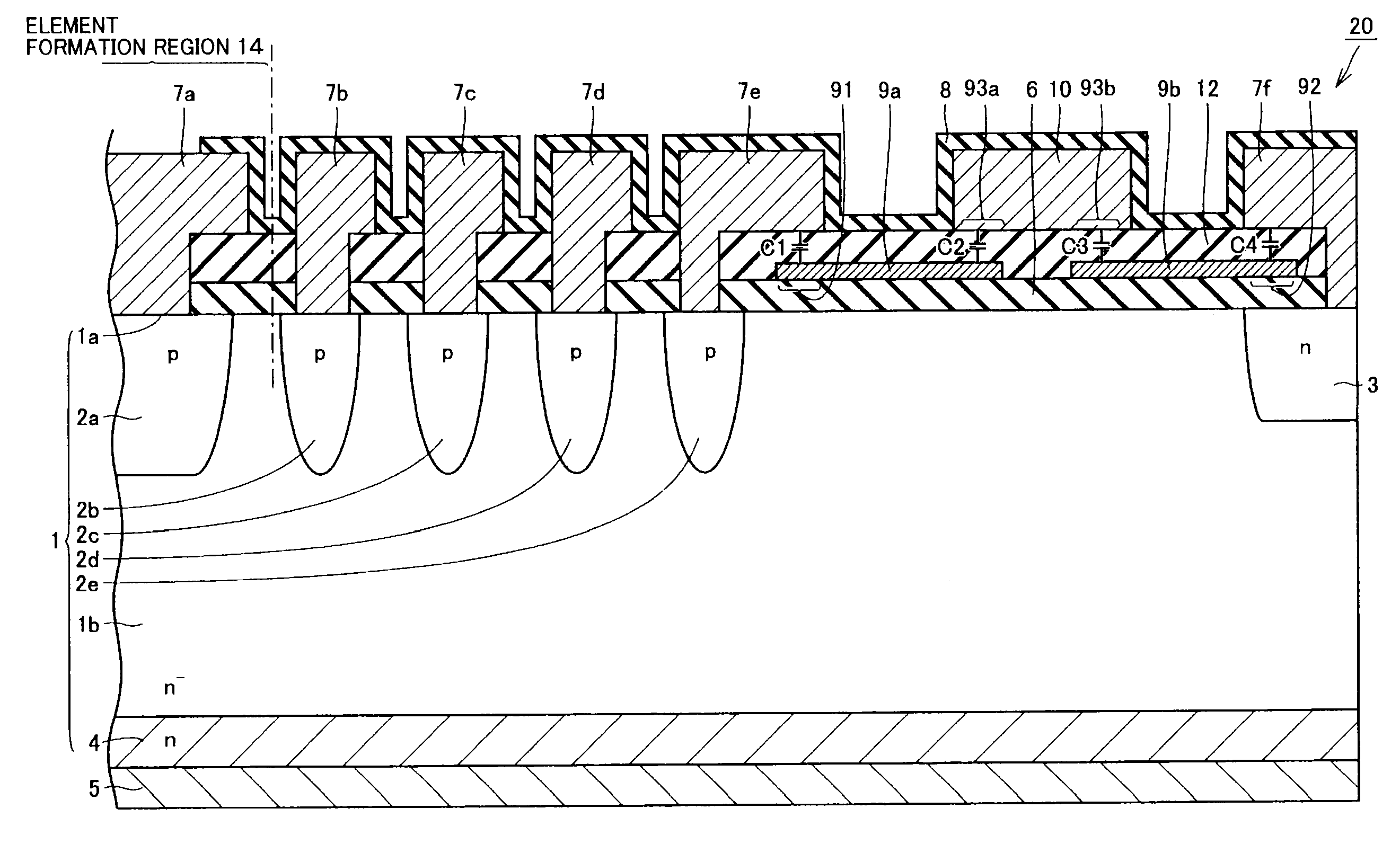
[0023]First, a configuration of a semiconductor device of a first embodiment of the present invention will be described.
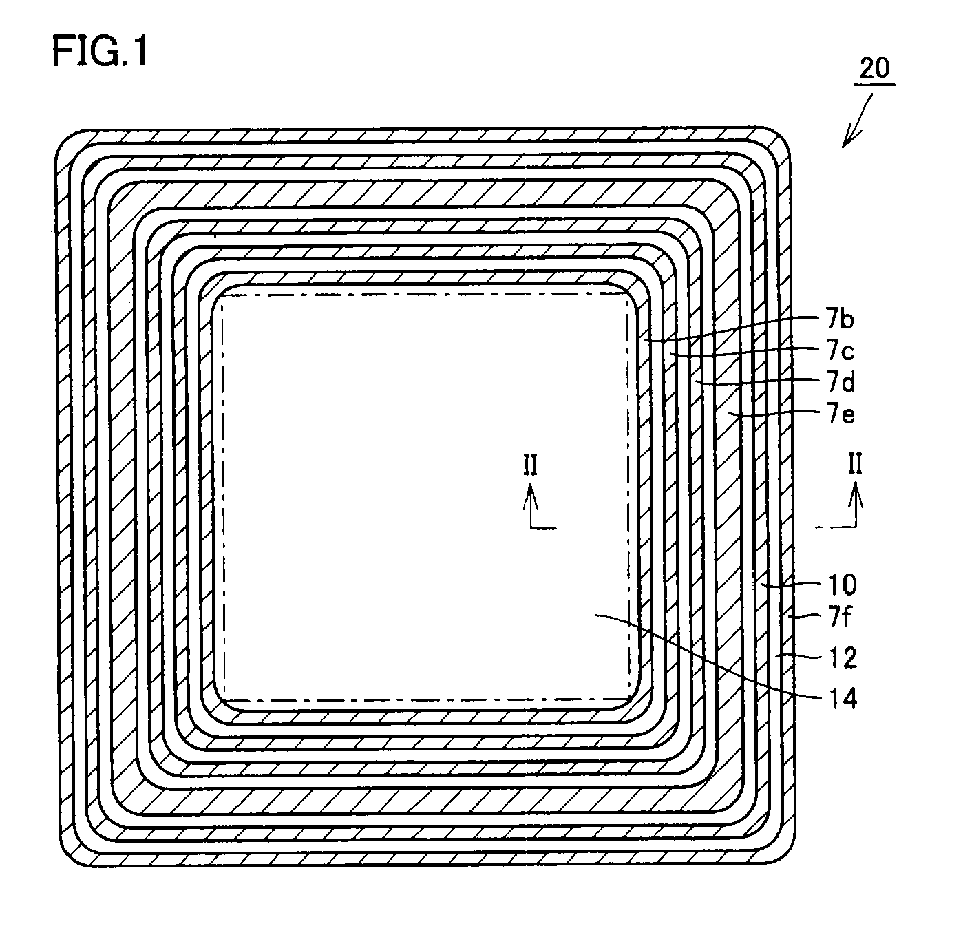
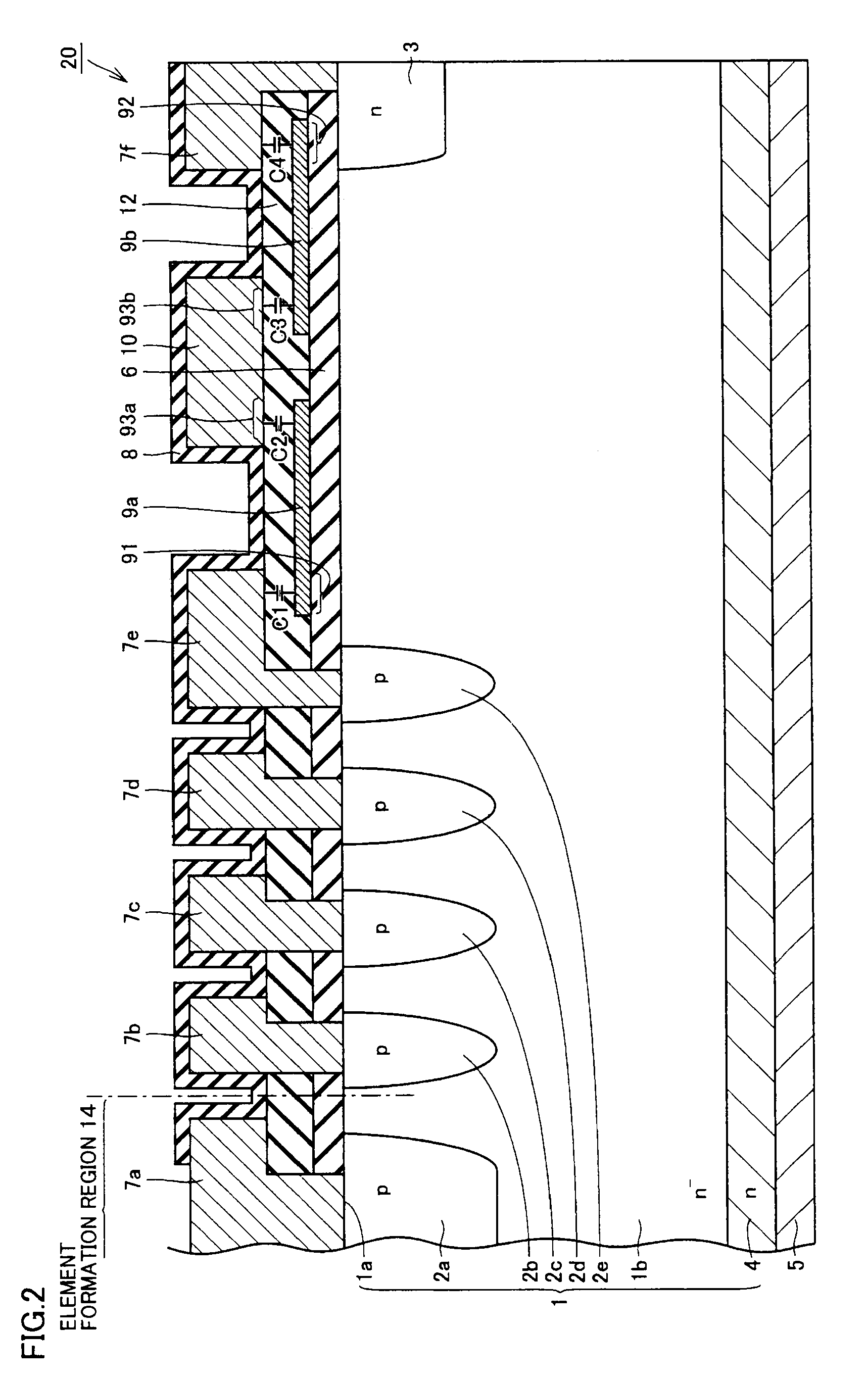
[0024]Referring to FIG. 1 and FIG. 2, semiconductor device 20 of the present embodiment mainly has a semiconductor substrate 1, a collector electrode 5, a field oxide film 6, an emitter electrode 7a, guard ring electrodes 7b, 7c, 7d, 7e, a channel stopper electrode 7f, and field plates 9a, 9b, 10. For visibility, a passivation film 8 is not drawn in FIG. 1.
[0025]Referring to mainly FIG. 1, when viewed in a plan view, semiconductor device 20 has a central portion provided with a formation region 14 for a power semiconductor element such as an IGBT (Insulated Gate Bipolar Transistor). When viewed in the plan view, guard ring electrodes 7b, 7c, 7d, 7e are formed to surround a circumference of element formation region 14. When viewed in the plan view, field plate 10 and channel stopper electrode 7f are formed to surround the circumference of guard ring electrode 7e.
[0...
second embodiment
[0053]A semiconductor device of a second embodiment of the present invention is different from the semiconductor device of the first embodiment mainly in configurations of field plates.
[0054]Referring to FIG. 3 and FIG. 4, semiconductor substrate 1 has a main surface 1a over which field plates 9a, 9b are formed with a field oxide film 6 interposed between main surface 1a and field plates 9a, 9b. For visibility, in FIG. 3, a passivation film 8 is not drawn.
[0055]Formed on field plates 9a, 9b is an insulation film 13 on which a field plate 9c (third portion) is formed. On field plate 9c, an interlayer insulation film 12 is formed. On interlayer insulation film 12, a guard ring electrode 7e and a channel stopper electrode 7f are formed. In other words, field plate 9c (third portion) is formed as a layer below guard ring electrode 7e and channel stopper electrode 7f.
[0056]When viewed in a plan view, field plate 9c (third portion) has a portion 93a overlapping with field plate 9a (first...
third embodiment
[0062]A semiconductor device of a third embodiment of the present invention is different from the semiconductor device of the first embodiment in configurations of field plates.
[0063]Referring to FIG. 5, semiconductor substrate 1 has a main surface 1a over which field plates 9a, 9b are formed with a field oxide film 6 interposed between main surface 1a and field plates 9a, 9b. Field plates 9c (third portion) are formed between field plates 9a, 9b and an interlayer insulation film 12 is provided among them. In the present embodiment, two field plates 9c (third portion) are described but the present invention is not limited to this. A single or a plurality of field plates 9c may be provided. Field plates 9a, 9b, 9c are arranged along a direction in which main surface 1a of semiconductor substrate 1 extends. Field plates 9a, 9b, 9c overlap with their adjacent field plates 9a, 9b, 9c in the direction in which main surface 1a extends.
[0064]In the direction in which main surface 1a extend...
PUM
 Abstract
Description
Claims
Application Information
 - R&D
- Intellectual Property
- Life Sciences
- Materials
- Tech Scout
- Unparalleled Data Quality
- Higher Quality Content
- 60% Fewer Hallucinations
Browse by: Latest US Patents, China's latest patents, Technical Efficacy Thesaurus, Application Domain, Technology Topic, Popular Technical Reports.
© 2025 PatSnap. All rights reserved.Legal|Privacy policy|Modern Slavery Act Transparency Statement|Sitemap|About US| Contact US: help@patsnap.com