
Solid-state image pickup apparatus and electronic apparatus

a pickup apparatus and solid-state image technology, applied in the field of solid-state image pickup apparatus and electronic apparatus, can solve the problems of reducing the size of a photoelectric converter as a photodiode, increasing the noise component with the increase in the number of pixels, and reducing the s/n ratio, so as to prevent the ripple and sensitivity deterioration, and preventing the fluctuation from affecting the image formation

Active Publication Date: 2010-09-30
SONY CORP
View PDF43 Cites 7 Cited by
  • Summary
  • Abstract
  • Description
  • Claims
  • Application Information

AI Technical Summary

Benefits of technology

[0006]In view of the above-mentioned circumstances, it is desirable to prevent the ripple and the deterioration of the sensitivity that depends on the wavelength in the solid-state image pickup apparatus of the back-surface irradiation type.
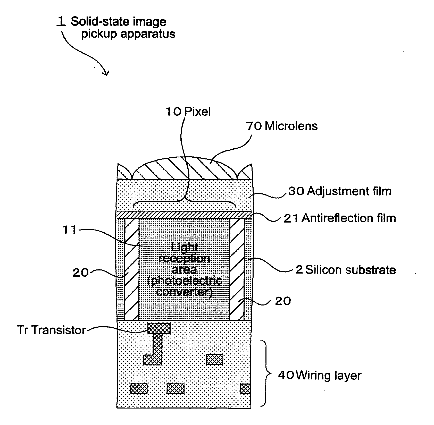
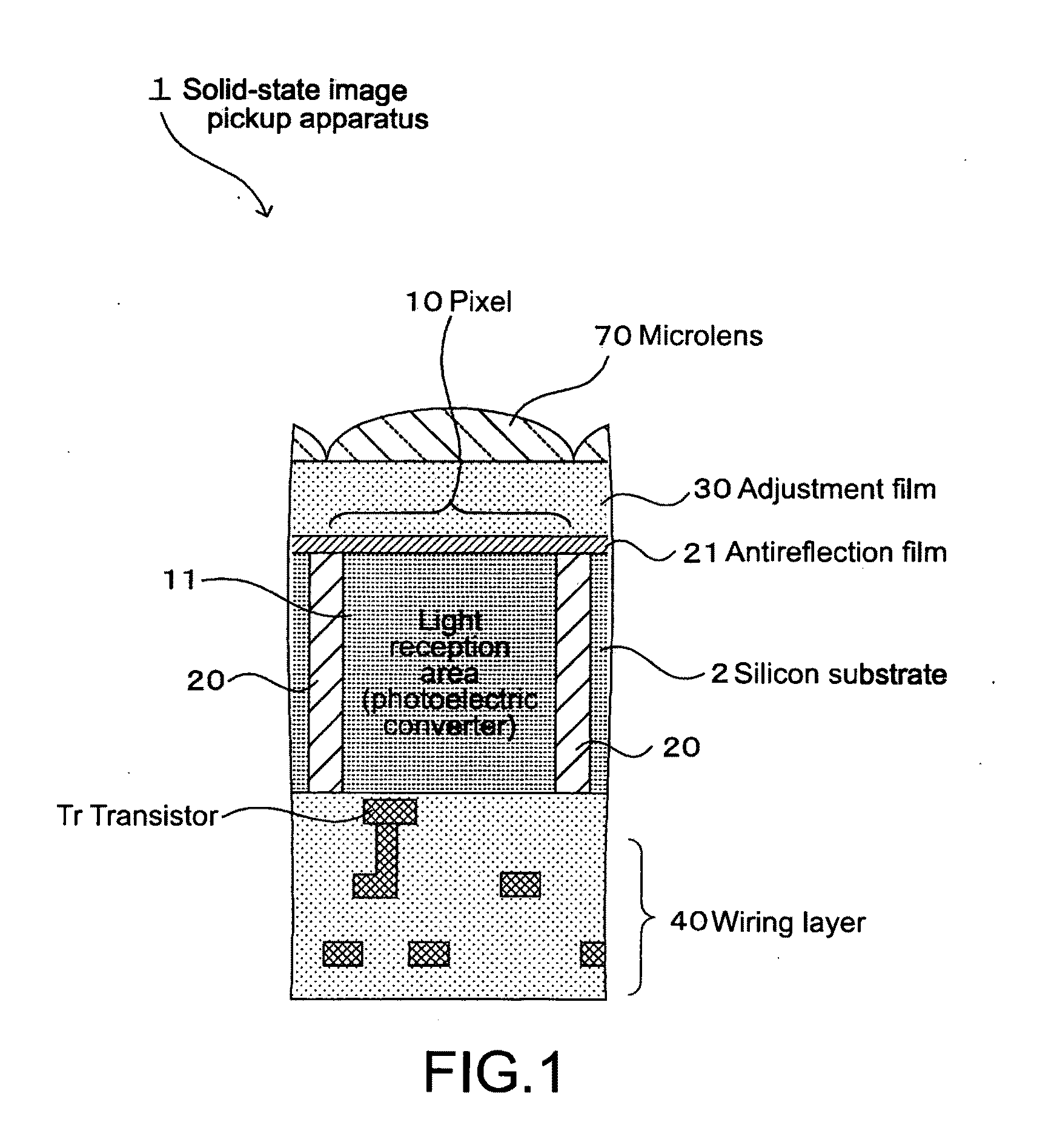
[0008]In the embodiment of the present invention, the adjustment film provided between the photoelectric converter and the micro lens adjusts the fluctuation of the light reception sensitivity in the photoelectric converter with respect to the wavelength of light that enters the photoelectric converter through the micro lens. Specifically, the adjustment is made so that the period of the variation of the average transmittance every 10-nm wavelengths of light is set to be smaller than a distance between a center wavelength (for example 540 nm) of blue light and a center wavelength (for example 450 nm) of green light. Thus, the fluctuation of the light reception sensitivity with respect to the wavelength is prevented from affecting the color balance.
[0010]According to the embodiment of the present invention, it is possible to prevent the ripple and the sensitivity deterioration that depends on the wavelength in the solid-state image pickup apparatus of a back-surface irradiation type. Further, even when the fluctuation of the light reception sensitivity with respect to the wavelength is caused, it is possible to prevent the fluctuation from affecting the image formation.

Problems solved by technology

In a solid-state image pickup apparatus, a noise component is increased with the increase in the number of pixels, so it becomes difficult to secure the same S / N ratio.
However, also in the CMOS image sensor of a back-surface irradiation type, the size of a photoelectric converter as a photodiode is reduced, and a sufficient sensitivity is difficult to be obtained.
Therefore, when a large ripple is found in a response spectrum, sensitivity deterioration is caused, and a balance of colors is lost, which causes a problem in forming an image.

Method used


Image

  • Solid-state image pickup apparatus and electronic apparatus
  • Solid-state image pickup apparatus and electronic apparatus
  • Solid-state image pickup apparatus and electronic apparatus

Examples


Embodiment Construction

[0023]Hereinafter, embodiments of the present invention will be described with reference to the drawings. The description will be given in order of the following items.

1. Outline of solid-state image pickup apparatus (structure having CMOS image sensor of back-surface irradiation type and color filter)

2. Features of embodiment (structure of adjustment film, structure impedance matching, thickness of silicon oxide, and structure of antireflection film)

3. Electronic apparatus (example of image pickup apparatus)

[0024]

[0025](CMOS Image Sensor of Back-Surface Irradiation Type)

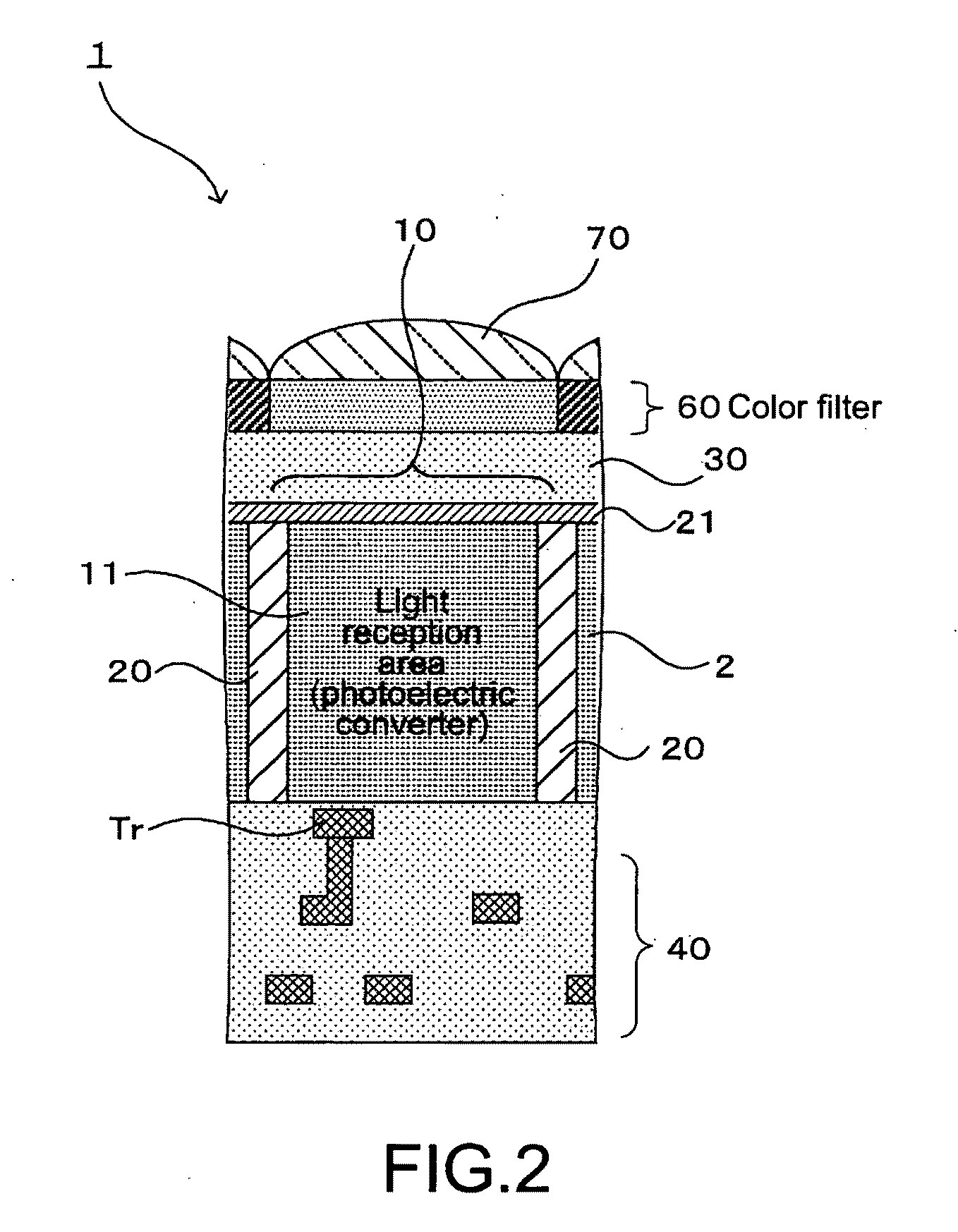
[0026]FIG. 1 is a schematic cross-sectional diagram for explaining an outline of a solid-state image pickup apparatus according to an embodiment. A solid-state image pickup apparatus 1 of this embodiment is a so-called CMOS image sensor of a back-surface irradiation type. In the solid-state image pickup apparatus 1, one side (upper side in FIG. 1) of a silicon substrate 2 in which a light reception area (photoelectr...


PUM


Abstract

A solid-state image pickup apparatus includes a photoelectric converter, a wiring portion, a micro lens, and an adjustment film. The photoelectric converter is formed on a light incident side in a substrate. The wiring portion is formed on a side of the substrate that is opposite to the light incident side. The micro lens is formed on a light incident side of the photoelectric converter. The adjustment film adjusts variation of a light reception sensitivity in the photoelectric converter with respect to a wavelength of light that enters the photoelectric converter through the micro lens, and the adjustment film is formed between the photoelectric converter and the micro lens.

Description

BACKGROUND OF THE INVENTION[0001]1. Field of the Invention[0002]The present invention relates to a solid-state image pickup apparatus and an electronic apparatus. In particular, the present invention relates to a solid-state image pickup apparatus including a photoelectric converter formed on a light incident side in a substrate and a wiring portion formed on a side opposite to the light incident side and having a film that adjusts light reception sensitivity in accordance with a wavelength on a light incident side of the photoelectric converter, and relates to an electronic apparatus.[0003]2. Description of the Related Art[0004]In a semiconductor image sensor typified by a CMOS (complementary metal oxide semiconductor) image sensor, the reduction in pixel size and the increase in number of pixels in the same image area are demanded. In Japanese Patent Application Laid-open No. 2008-270679 (hereinafter, referred to as Patent Document 1), there has been disclosed a technique of reduc...

Claims


Application Information

Patent Timeline
Patent Type & Authority Applications(United States)
IPC IPC(8): H04N5/335H01L27/14H04N25/00
CPCH01L27/14621H01L27/14627H01L27/1464H04N5/2257H04N5/2254H01L27/14623H04N23/57
Inventor KIKUCHI, KOJI
Owner SONY CORP
Learn More