
High light-extraction efficiency light-emitting diode structure

a light-emitting diode, high-efficiency technology, applied in the direction of basic electric elements, electrical appliances, semiconductor devices, etc., can solve the problems of unnecessary light loss, unfavorable light extraction efficiency, peeling off, etc., to achieve high-reflectivity and peeling-free, light extraction efficiency is increased, and light loss is reduced.

Inactive Publication Date: 2010-09-30
HIGH POWER OPTO
View PDF4 Cites 4 Cited by
  • Summary
  • Abstract
  • Description
  • Claims
  • Application Information

AI Technical Summary

Benefits of technology

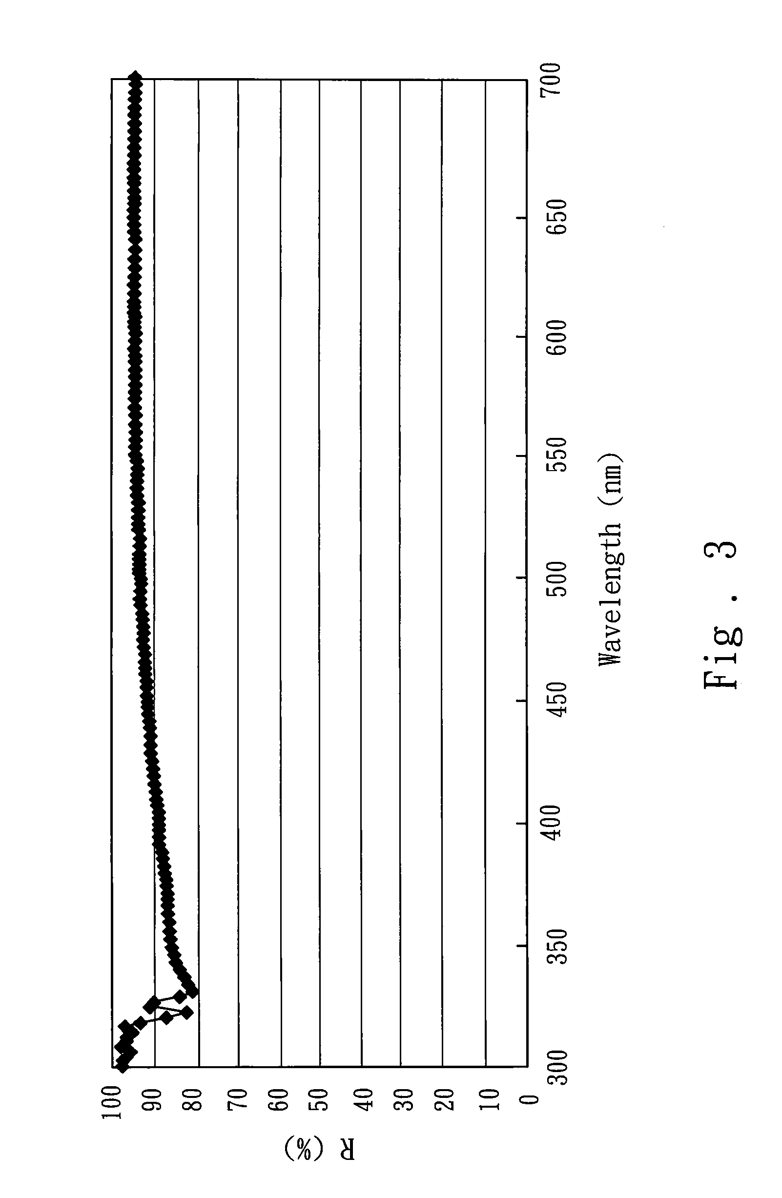
The present invention aims to create LED structures that have high light-extraction efficiency, meaning that more light is reflected and conducted by the metallic pads and metallic mesh wires, reducing light loss and increasing brightness. This is achieved by using an aluminum-silver alloy as the electric-conduction layer, which has high reflectivity in the visible spectra. This results in increased efficiency of LED, decreased waste heat, lower temperature, and prolonged service life.

Problems solved by technology

However, ITO has a problem of peel-off and is likely to react with silver.
When cooperating with silver, the nickel / gold or chromium / gold has a reflectivity of only 50-60%, absorbs a considerable amount of light, and results in an unneglectable light loss, which not only decreases the brightness of LED but also generates waste heat.
Thus, the service life of LED is decreased by high temperature.

Method used


Image

  • High light-extraction efficiency light-emitting diode structure
  • High light-extraction efficiency light-emitting diode structure
  • High light-extraction efficiency light-emitting diode structure

Examples


Embodiment Construction

[0011]The technical contents of the present invention will be described in detail with the embodiments. However, it should be understood that the embodiments are only to exemplify the present invention but not to limit the scope of the present invention.

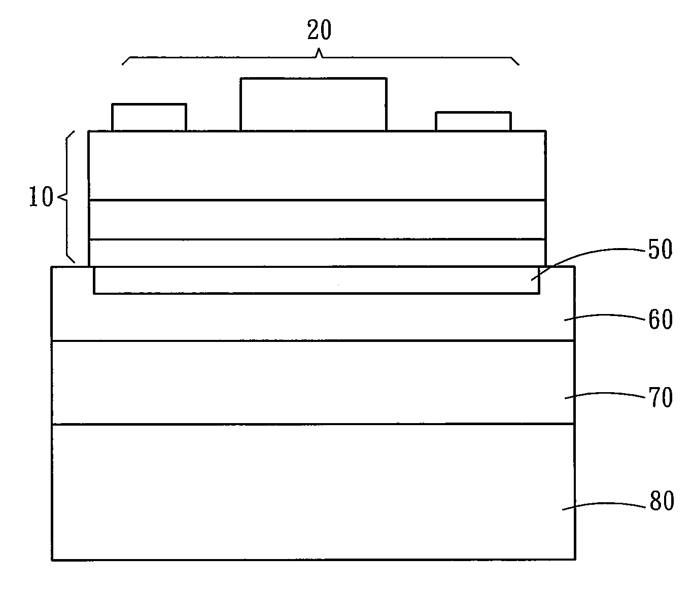
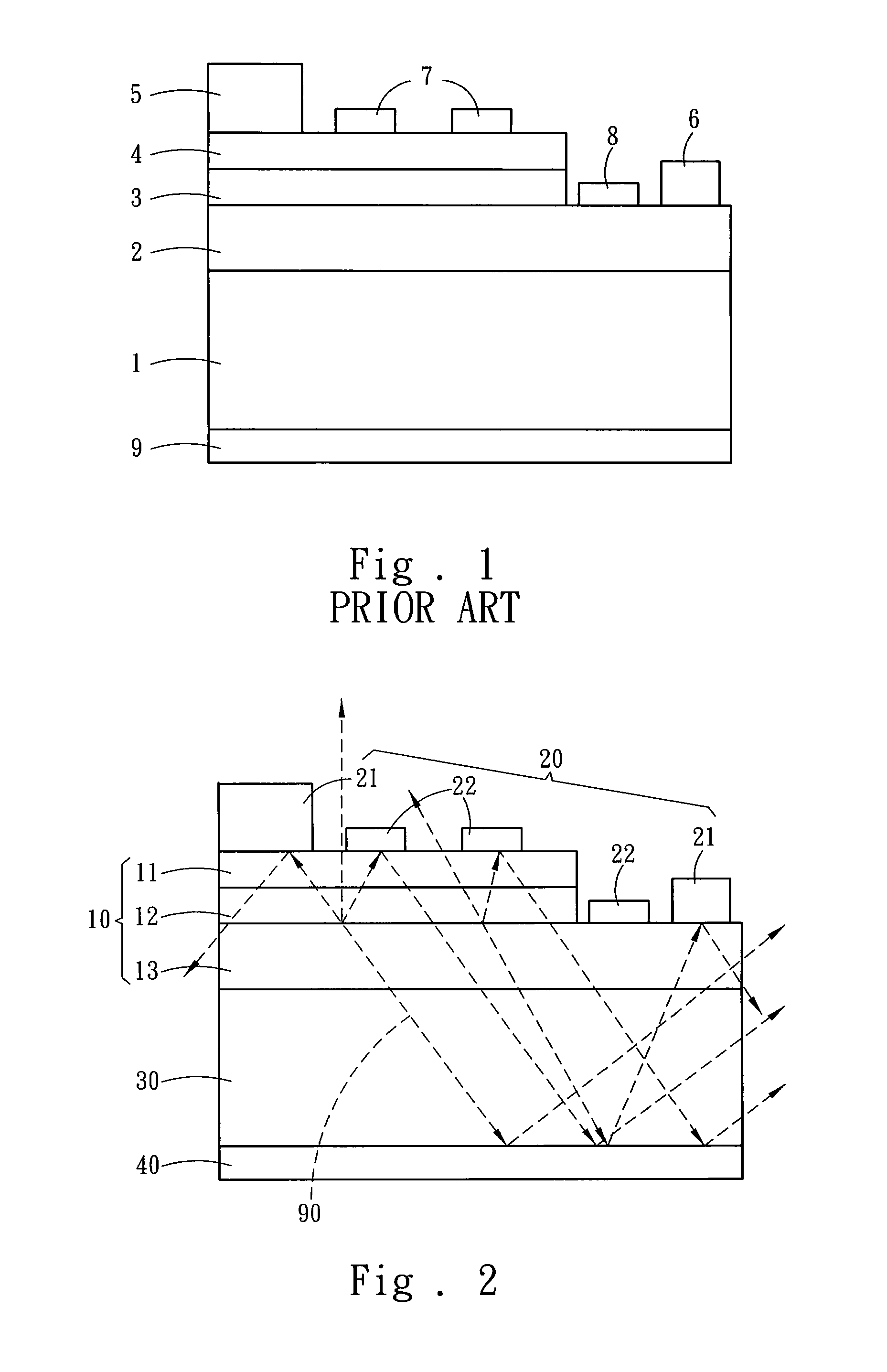
[0012]Refer to FIG. 2 for a first embodiment of the present invention. In the first embodiment, the high light-extraction efficiency light-emitting diode structure of the present invention comprises an LED epitaxial layer 10 and at least one electric-conduction layer 20 formed over the LED epitaxial layer 10. The LED epitaxial layer 10 includes a hole supply layer 11, an active layer 12 and an electron supply layer 13, which are stacked sequentially. The electric-conduction layer 20 is fabricated via forming an aluminum layer having a thickness of 10-50 nm and a silver layer having a thickness of 80-500 nm and tempering the two layers at a high temperature to form an aluminum-silver alloy. The electric-conduction layer 20 can be fabr...


PUM

PropertyMeasurementUnit
thicknessaaaaaaaaaa
thicknessaaaaaaaaaa
reflectivityaaaaaaaaaa

Abstract

The present invention discloses a high light-extraction efficiency LED structure, wherein metallic pads and metallic mesh wires made of an aluminum-silver alloy are formed on an LED, whereby the high-reflectivity aluminum-silver alloy makes the light incident on the metallic pads and metallic mesh wires reflected once more or repeatedly and then emitted from the surface or lateral side of the LED, wherefore the present invention can decrease the light loss and increase the light-extraction efficiency.

Description

FIELD OF THE INVENTION[0001]The present invention relates to a light-emitting diode structure, particularly to a high light-extraction efficiency light-emitting diode structure.BACKGROUND OF THE INVENTION[0002]Refer to FIG. 1 for a conventional light-emitting diode (LED), wherein an N-type gallium nitride layer (n-GaN) 2, a multi-layer quantum well (MQW) 3, a P-type gallium nitride (p-GaN) 4 are sequentially epitaxially grown on a substrate 1; then a P-type metallic pad (p-Pad) 5 and an N-type metallic pad (n-Pad) 6 are coated on the abovementioned epitaxial layers. If the LED is to be used as a high-power and large-size LED, metallic mesh wires 7 and 8 are simultaneously coated on the epitaxial layers during coating the P-type metallic pad 5 and the N-type metallic pad 6. For a high-power and large-size LED, a high-reflectivity reflecting layer 9 is further coated on the grinded and polished substrate 1 to increase the brightness of the LED by reflection.[0003]In a high-power and l...

Claims


Application Information

Patent Timeline
Patent Type & Authority Applications(United States)
IPC IPC(8): H01L33/00
CPCH01L33/405
Inventor YAN, LIANG-JYICHIANG, CHANG-HANLEE, YEA-CHENCHANG, CHIH-SUNG
Owner HIGH POWER OPTO
Learn More