Solid-state imaging apparatus and method for driving the same
a technology of solid-state imaging and imaging apparatus, which is applied in the direction of color television details, television system details, television systems, etc., can solve the problems of narrowed dynamic range of column amplifiers and saturated output, and achieve high s/n ratio in each operation mode, suitable dynamic range
- Summary
- Abstract
- Description
- Claims
- Application Information
AI Technical Summary
Benefits of technology
Problems solved by technology
Method used
Image

Examples
first embodiment
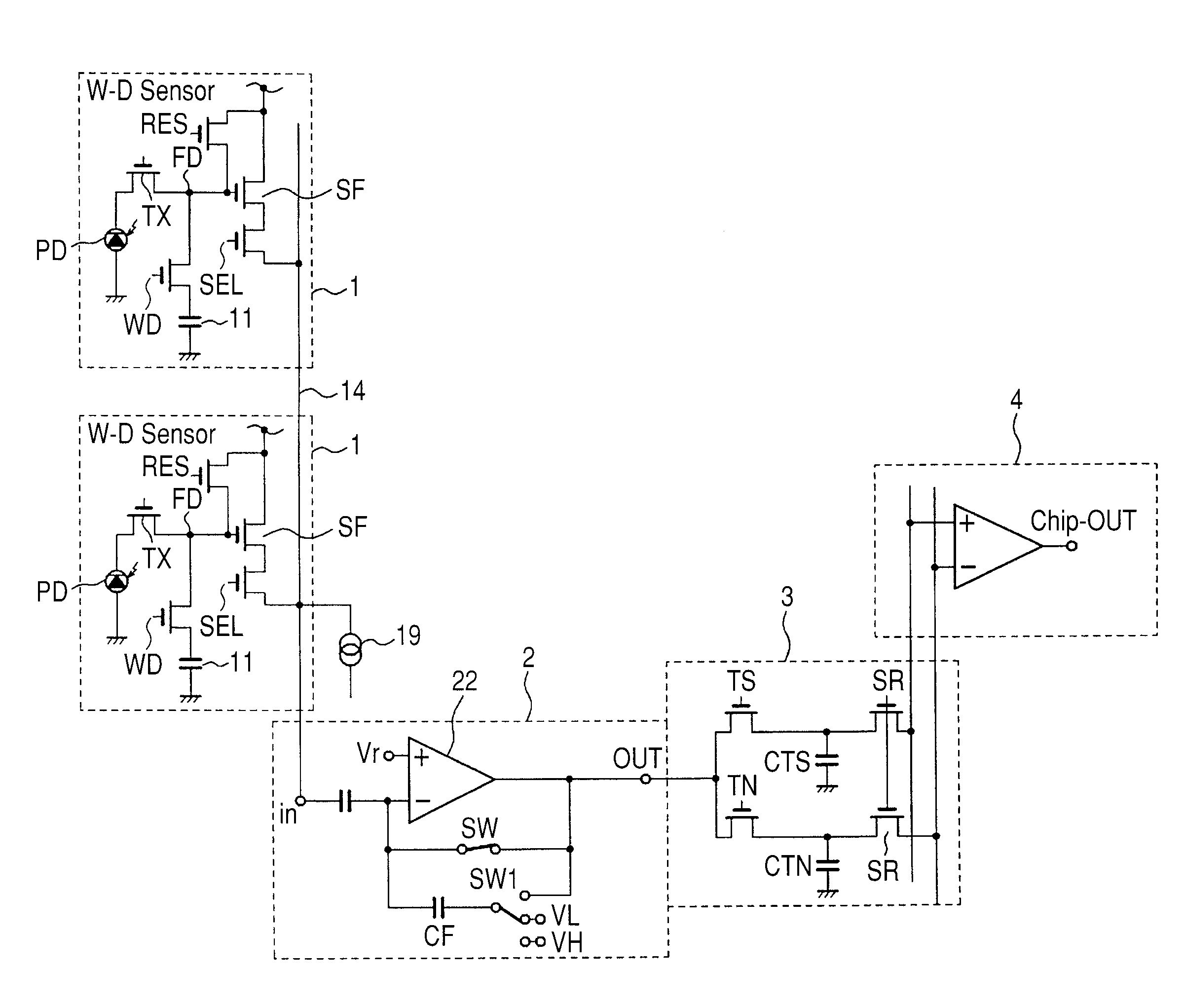
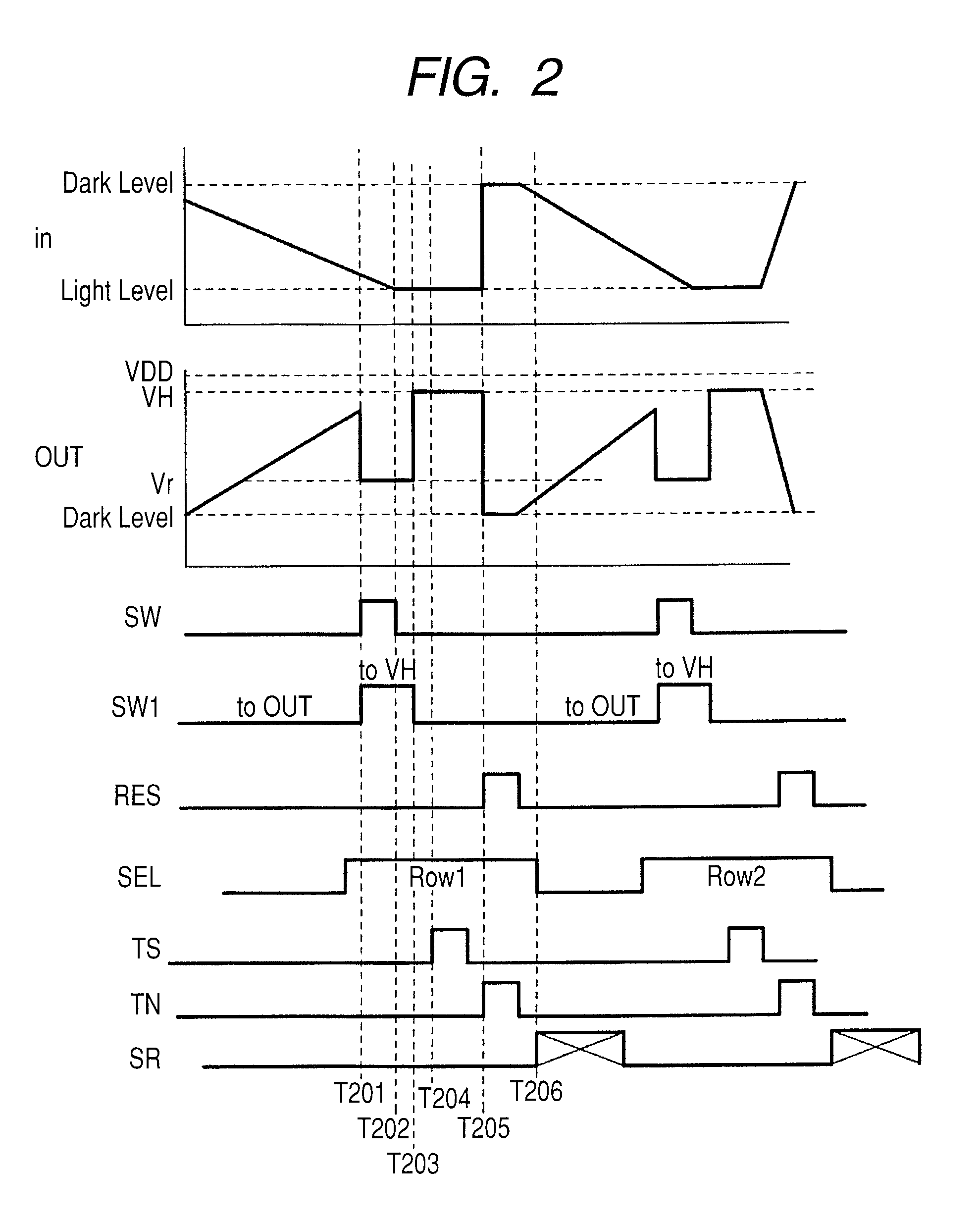
[0023]FIG. 1 is a circuit diagram illustrating an example configuration of a solid-state imaging apparatus according to a first embodiment of the present invention, which illustrates circuits for two pixels in a certain column and a read out circuit connected to a signal output line 14, to which these two pixels are connected in common, from the solid-state imaging apparatus in which pixels are two-dimensionally arranged.
[0024]Pixels (sensor and pixel circuits) 1 are pixels enabling provision of a wide dynamic range. Each pixel 1 includes a photoelectric conversion unit PD, an output source follower transistor SF, a capacitor 11 for a wide dynamic range, a switch WD, a pixel signal transfer switch TX, a pixel reset switch RES and a row selection switch SEL. FIG. 1 illustrates a signal output line 14 and a current source 19 as well. The photoelectric conversion unit PD, which may be, for example, a photo diode, generates a charge by photoelectric conversion and accumulate the charge....
second embodiment
[0049]In the first embodiment, a description has individually been provided for a dynamic range expansion operation and a normal operation. Meanwhile, for a second embodiment of the present invention, an example in which a normal operation to read out a charge accumulated in a photoelectric conversion unit PD is performed subsequent to a dynamic range expansion operation.
[0050]FIG. 5 is an equivalent circuit diagram of a pixel in a second embodiment of the present invention, and FIG. 6 is a circuit diagram illustrating an example configuration of a solid-state imaging apparatus according to a second embodiment of the present invention. A pixel is configured as illustrated in FIG. 5, and is different from the first embodiment in that it does not include the switch WD and the capacitor 11. The solid-state imaging apparatus is configured as illustrated in FIG. 6, and is provided with two sets of capacitors: capacitors CTSW and CTNW for holding a signal obtained as a result of a dynamic...
PUM
 Abstract
Description
Claims
Application Information
 - R&D
- Intellectual Property
- Life Sciences
- Materials
- Tech Scout
- Unparalleled Data Quality
- Higher Quality Content
- 60% Fewer Hallucinations
Browse by: Latest US Patents, China's latest patents, Technical Efficacy Thesaurus, Application Domain, Technology Topic, Popular Technical Reports.
© 2025 PatSnap. All rights reserved.Legal|Privacy policy|Modern Slavery Act Transparency Statement|Sitemap|About US| Contact US: help@patsnap.com