
Method of improving surface morphology of (ga,al,in,b)n thin films and devices grown on nonpolar or semipolar (ga,al,in,b)n substrates

a technology of nonpolar or semipolar nitride and thin film, which is applied in the direction of semiconductor lasers, lasers, transportation and packaging, etc., can solve the problems of inherently large effective hole mass and detrimental electric fields, and achieve the effects of improving surface morphology, improving surface smoothness, and improving growth morphology

Inactive Publication Date: 2010-09-02
RGT UNIV OF CALIFORNIA
View PDF13 Cites 18 Cited by
  • Summary
  • Abstract
  • Description
  • Claims
  • Application Information

AI Technical Summary

Benefits of technology

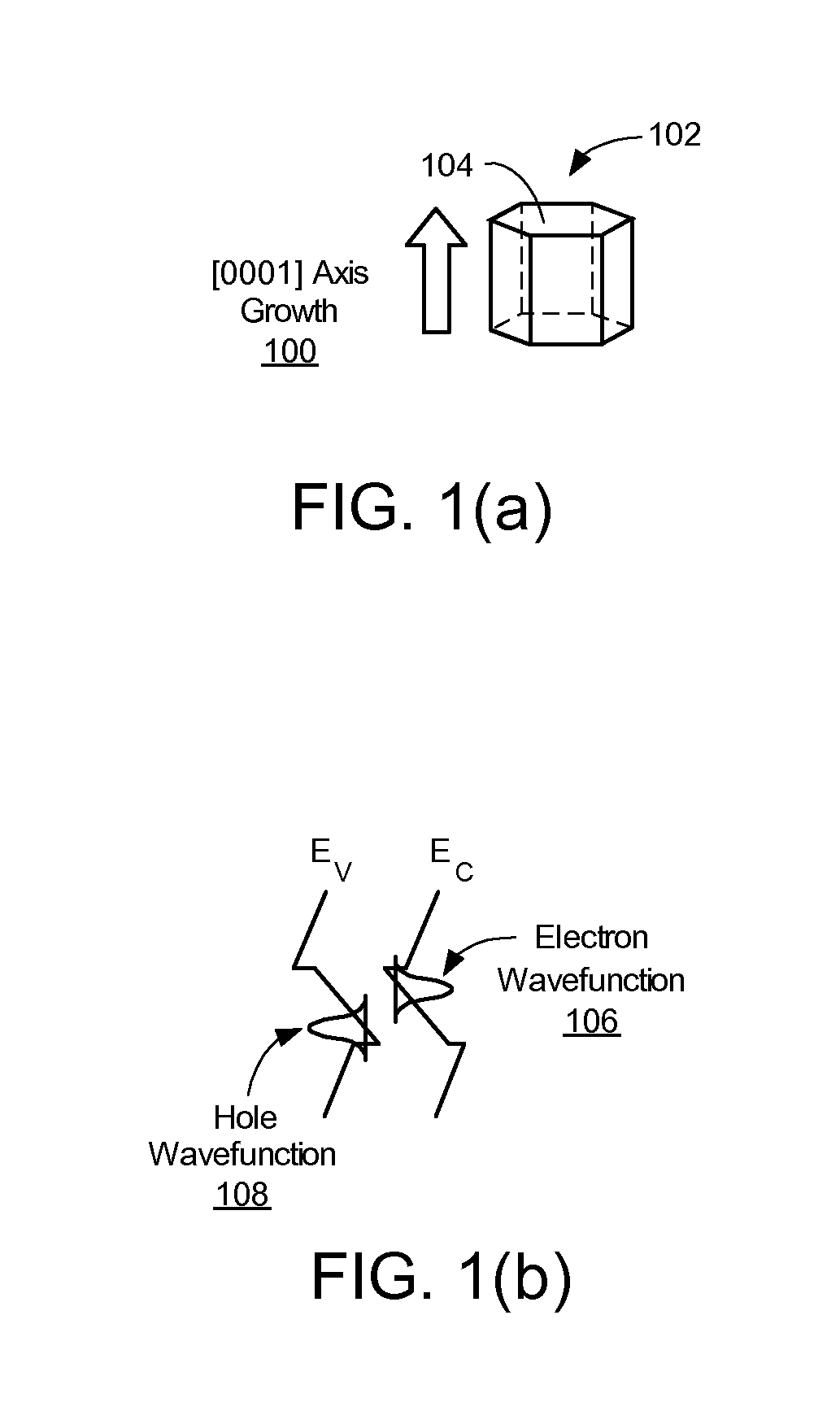
[0024]Growth of nonpolar or semipolar nitride thin films and heterostructures offers a means of decreasing polarization effects and reducing the effective hole mass in würtzite nitride device structures. The terms “nitrides,”“(Ga,Al,In,B)N”, or “III-Nitride” refers to any alloy composition of the (Ga,Al,In,B)N semiconductors having the formula Gaw,AlxInyBzN where 0≦w≦1, 0≦x≦1, 0≦y≦1, 0≦z≦1, and w+x+y+z=1. Current commercially-available LEDs and diode lasers are grown along the polar [0001] c-direction. The associated polarization-induced electric fields and the inherently large effective hole mass are detrimental to the performance of state-of-the-art nitride LEDs and diode lasers. Growth of these devices on nonpolar or semipolar planes can significantly improve device performance by decreasing polarization-induced electric fields and reducing the effective hole mass.
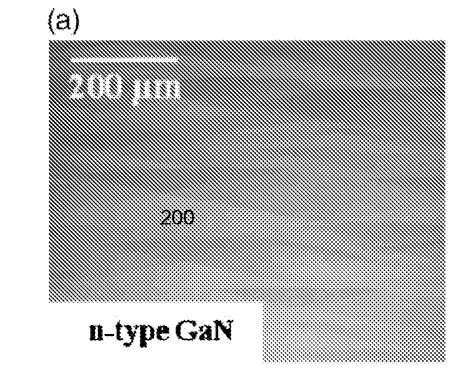
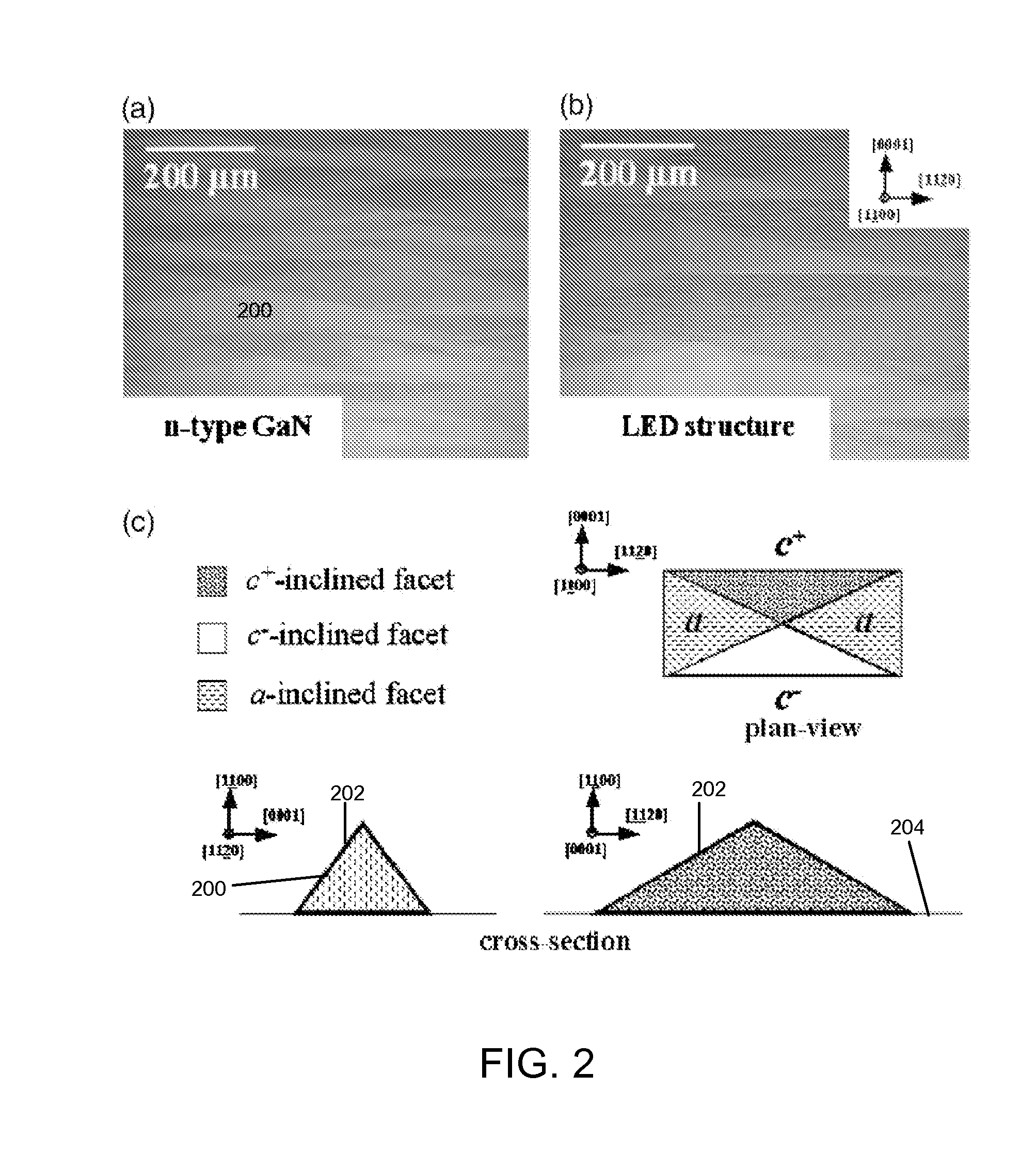
[0026]This invention describes a method for improving the growth morphology of (Ga,Al,In,B)N thin films on nonpolar or semipolar (Ga,Al,In,B)N substrates by using an inert carrier gas such as N2. For example, the present invention is able to improve surface smoothness of nonpolar and semipolar films as compared to films grown in [Refs. 2-4].
[0027]Improved surface morphology can lead to a number of advantages for nonpolar or semipolar nitride device manufacturers, including, but not limited to, better uniformity in the thickness, composition, doping, electrical properties, and luminescence characteristics of individual layers in a given device. Furthermore, smooth surfaces can be especially beneficial for nonpolar or semipolar nitride laser diodes, leading to significant reductions in optical scattering losses.

Problems solved by technology

The associated polarization-induced electric fields and the inherently large effective hole mass are detrimental to the performance of state-of-the-art nitride LEDs and diode lasers.

Method used


Image

  • Method of improving surface morphology of (ga,al,in,b)n thin films and devices grown on nonpolar or semipolar (ga,al,in,b)n substrates
  • Method of improving surface morphology of (ga,al,in,b)n thin films and devices grown on nonpolar or semipolar (ga,al,in,b)n substrates
  • Method of improving surface morphology of (ga,al,in,b)n thin films and devices grown on nonpolar or semipolar (ga,al,in,b)n substrates

Examples


Embodiment Construction

[0050]In the following description of the preferred embodiment, reference is made to the accompanying drawings which form a part hereof, and in which is shown by way of illustration a specific embodiment in which the invention may be practiced. It is to be understood that other embodiments may be utilized and structural changes may be made without departing from the scope of the present invention.

[0051]Overview

[0052]The realization of nonpolar or semipolar nitride LEDs and diode lasers allows for multiple advances in the manufacturability of nitride LEDs and diode lasers. Growth of nitride LEDs and diode lasers on a nonpolar or semipolar planes can significantly improve device performance by decreasing polarization-induced electric fields and reducing the effective hole mass through anisotropic strain-induced splitting of the heavy hole and light hole bands. Decreasing polarization-induced electric fields can increase the radiative efficiency in nitride LEDs. Likewise, decreasing po...


PUM

PropertyMeasurementUnit
miscut angleaaaaaaaaaa
surface roughnessaaaaaaaaaa

Abstract

A method for improving the growth morphology of (Ga,Al,In,B)N thin films on nonpolar or semipolar (Ga,Al,In,B)N substrates, wherein a (Ga,Al,In,B)N thin film is grown directly on a nonpolar or semipolar (Ga,Al,In,B)N substrate or template and a portion of the carrier gas used during growth is comprised of an inert gas. Nonpolar or semipolar nitride LEDs and diode lasers may be grown on the smooth (Ga,Al,In,B)N thin films grown by the present invention.

Description

CROSS-REFERENCE TO RELATED APPLICATION[0001]This application claims the benefit under 35 U.S.C. Section 119(e) of the following co-pending and commonly assigned U.S. Provisional Patent Applications:[0002]U.S. Provisional Patent Application Ser. No. 61 / 156,710, filed on Mar. 2, 2009, by Robert M. Farrell, Michael Iza, James S. Speck, Steven P. DenBaars, and Shuji Nakamura, entitled “METHOD OF IMPROVING SURFACE MORPHOLOGY OF (Ga,Al,In,B)N THIN FILMS AND DEVICES GROWN ON NONPOLAR OR SEMIPOLAR (Ga,Al,In,B)N SUBSTRATES,” attorney's docket number 30794.306-US-P1 (2009-429-1); and[0003]U.S. Provisional Patent Application Ser. No. 61 / 184,535, filed on Jun. 5, 2009, by Robert M. Farrell, Michael Iza, James S. Speck, Steven P. DenBaars, and Shuji Nakamura, entitled “METHOD OF IMPROVING SURFACE MORPHOLOGY OF (Ga,Al,In,B)N THIN FILMS AND DEVICES GROWN ON NONPOLAR OR SEMIPOLAR (Ga,Al,In,B)N SUBSTRATES,” attorney's docket number 30794.306-US-P2(2009-429-2);[0004]which applications are incorporate...

Claims


Application Information

Patent Timeline
Patent Type & Authority Applications(United States)
IPC IPC(8): H01L29/20H01L21/20
CPCH01L21/02389H01L21/02433H01L21/0254H01L21/0262H01L33/007Y10T428/31H01L21/02609H01L33/005H01L33/32H01S5/343H01L33/18H01L21/20
Inventor FARRELL, ROBERT M.IZA, MICHAELSPECK, JAMES S.DENBAARS, STEVEN P.NAKAMURA, SHUJI
Owner RGT UNIV OF CALIFORNIA
Learn More