
Display apparatus

a technology of display apparatus and display screen, which is applied in the direction of instruments, discharge tube luminescnet screens, static indicating devices, etc., can solve the problem of increasing the width of the common line and the common line of the cathode to reduce the wiring resistance, increasing the voltage drop across the wire, and requiring the wire width to decrease, so as to achieve a high occupancy ratio of the light emitting area and high contrast display

Active Publication Date: 2010-08-26
OKI ELECTRIC IND CO LTD
View PDF5 Cites 9 Cited by
  • Summary
  • Abstract
  • Description
  • Claims
  • Application Information

AI Technical Summary

Benefits of technology

[0007]However, in such a conventional display apparatus, since the bare chip LED mounting areas are provided in areas other than the anode common lines and the cathode common lines, the wire line width is limited by the bare chip LED mounting areas so that the width of the anode common lines and the cathode common lines cannot be widened to reduce the wiring resistance. To achieve reduction of the wire resistance, the area for light emission becomes extremely small.
[0010]Therefore, with such a conventional display apparatus, it has been extremely difficult to realize greater density of light emitting elements and a smaller voltage drop across the connecting wires.

Problems solved by technology

However, in such a conventional display apparatus, since the bare chip LED mounting areas are provided in areas other than the anode common lines and the cathode common lines, the wire line width is limited by the bare chip LED mounting areas so that the width of the anode common lines and the cathode common lines cannot be widened to reduce the wiring resistance.
On the other hand, if the bare chip LED mounting area is enlarged, the width of the anode common lines and the cathode common lines must be decreased thereby resulting in a higher voltage drop across the wires and uneven brightness over the entire display.
Further, if increasing the density of bare chip LEDs is desired, the bare chip LED mounting area must be increased making it difficult to maintain the area for the anode common lines and the cathode common lines, thereby requiring the wire width to decrease.
Therefore, with such a conventional display apparatus, it has been extremely difficult to realize greater density of light emitting elements and a smaller voltage drop across the connecting wires.

Method used


Image

  • Display apparatus
  • Display apparatus
  • Display apparatus

Examples


first embodiment

Effect of First Embodiment

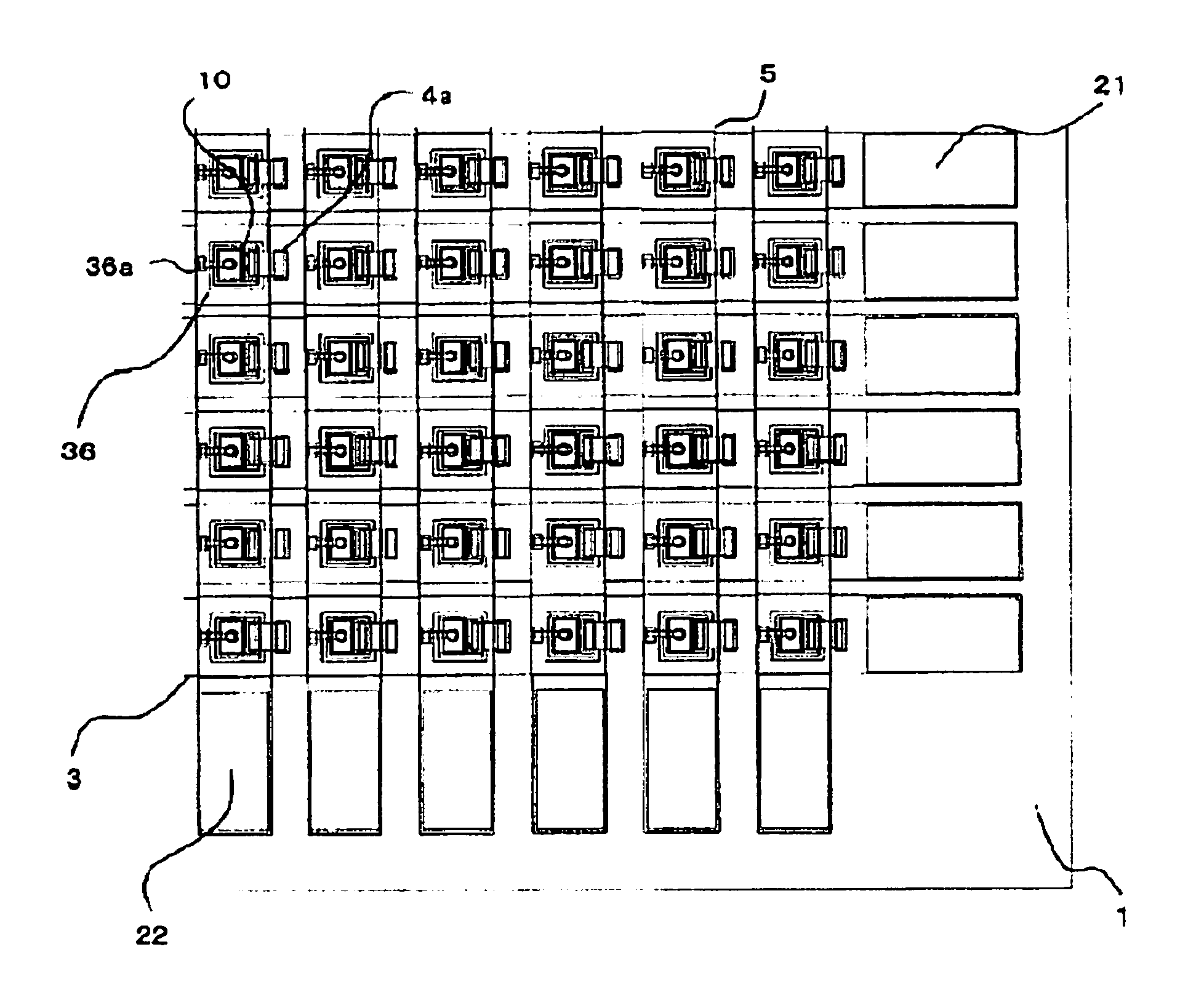
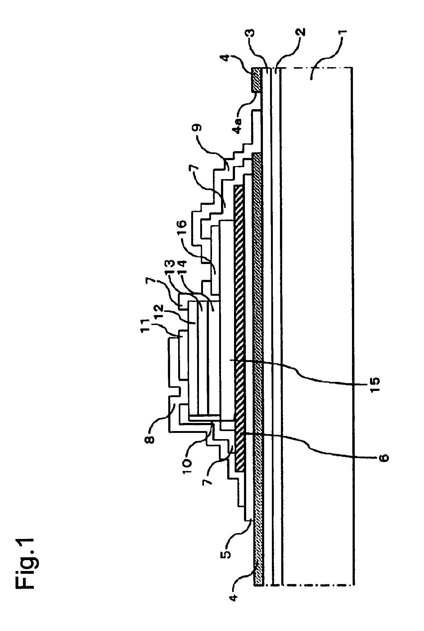
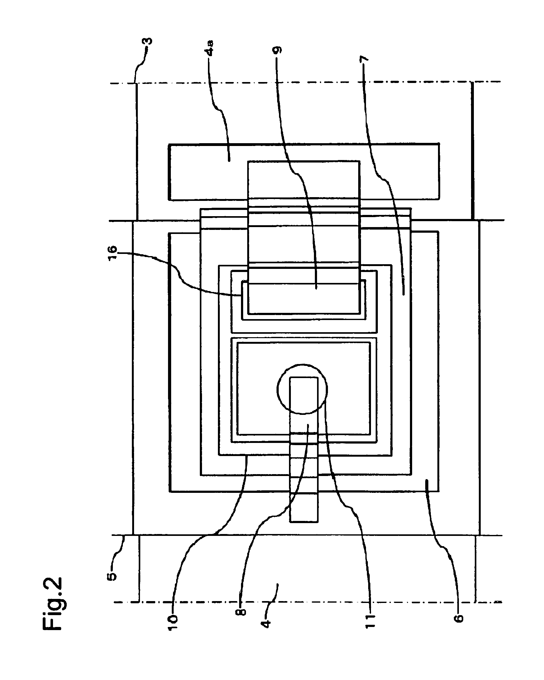
[0039]The typical surface roughness of a thin film wire formed by a vapor deposition method, a sputtering method or the like is generally greater than 5 nm, so it is difficult to mount semiconductor thin film LEDs 10 directly onto the intersection of lower electrode common line 3 and upper electrode common line 5 by using an intermolecular force. In the first embodiment, planarizing insulating film 6, whose surface has a typical roughness equal or less than 5 nm, is formed on the intersection of lower electrode common line 3 and upper electrode common line 5 to planarize the intersection, and semiconductor thin film LED 10 is three-dimensionally mounted on planarizing insulating film 6 by using an intermolecular force. With this configuration, the following effects (a) to (c) can be obtained.[0040](a) The width of each lower electrode common line 3 and upper electrode common line 5 can be increased regardless of the size of the area for mounting semiconduct...

second embodiment

Effect of Second Embodiment

[0051]According to the second embodiment, it is possible to manufacture a display apparatus that maximizes the area for forming lower electrode common lines 3 and upper electrode common lines 5 while maintaining a high occupancy ratio of the LED light emitting area. Thus, it is possible to manufacture a high-definition, high-intensity and large-screen display apparatus using semiconductor thin film LEDs 10. Further, since substantially the entire area around semiconductor thin film LED 10 is covered by light-block planarizing insulating film 36, a high-contrast display apparatus can be obtained.

modification examples

[0052]The invention is not limited to the first and second embodiments described above and various applications and modifications can be made. The following (a) to (c) are examples of the applications and modifications.

[0053](a) Although column-direction lines 5 are provided above row-direction lines 3 in the first and second embodiment, positions of column-direction lines 5 and row-direction line 3 in the stacking direction may be changed with each other such that row-direction lines 3 are provided above column-direction lines 5 and planarizing insulating film 6 or 36 is formed on above-located row-direction line 3. Modification (a) results in substantially the same effects as those of the first and second embodiments.

[0054](b) The configuration and shape of the display apparatus may be different from those shown in the drawings.

[0055](c) The materials of each element of the display apparatus and the manufacturing method of the display apparatus may be different from those of the f...


PUM


Abstract

A high-definition, high-intensity display apparatus having a plurality of semiconductor thin film light emitting elements and a plurality of linear electrodes connecting a power source to the light emitting elements, the linear electrodes being disposed so as to minimize the voltage drop across the linear electrodes.

Description

CROSS REFERENCE TO RELATED APPLICATIONS[0001]This application claims priority based on 35 USC 119 from prior Japanese Patent Application No. P2009-040422 filed on Feb. 24, 2009, entitled “DISPLAY APPARATUS”, the entire content of which is incorporated herein by reference.BACKGROUND OF THE INVENTION[0002]1. Field of the Invention[0003]The invention relates to a display apparatus including a matrix of semiconductor thin film light emitting elements integrated on a substrate.[0004]2. Description of Related Art[0005]Conventionally, in high-definition LED display apparatus using light emitting diodes (hereinafter, referred to as “LED”), that have very small pixel pitch of 3 mm or less bare chip LEDs are mounted in a two dimensional array (for example, Japanese Patent Application Laid-Open No. 2002-261335).[0006]Specifically, a matrix of anode common lines and cathode common lines is formed on a substrate. Bare chip LED mounting areas are provided in areas other than the anode common line...

Claims


Application Information

Patent Timeline
IPC IPC(8): G09G3/32
CPCG09G3/32G09G2300/0426H01L2924/12041H01L24/82H01L25/0753H01L33/62H01L2924/01013H01L2924/01029H01L2924/01079H01L2924/01005H01L2924/01006H01L2924/01033H01L2924/01078H01L2924/10329H01L24/24H01L2224/73267H01L2924/00
Inventor SUZUKI, TAKAHITOIGARI, TOMOKI
Owner OKI ELECTRIC IND CO LTD
Learn More