Voltage mode switching regulator and control circuit and method therefor
a voltage mode switching and control circuit technology, applied in the direction of ignition automatic control, process and machine control, instruments, etc., can solve the problems of low load current, extremely limited power conversion from the input to the output, and low load efficiency, so as to improve the light load efficiency and the effect of mode transition characteristi
- Summary
- Abstract
- Description
- Claims
- Application Information
AI Technical Summary
Benefits of technology
Problems solved by technology
Method used
Image
Examples
first embodiment
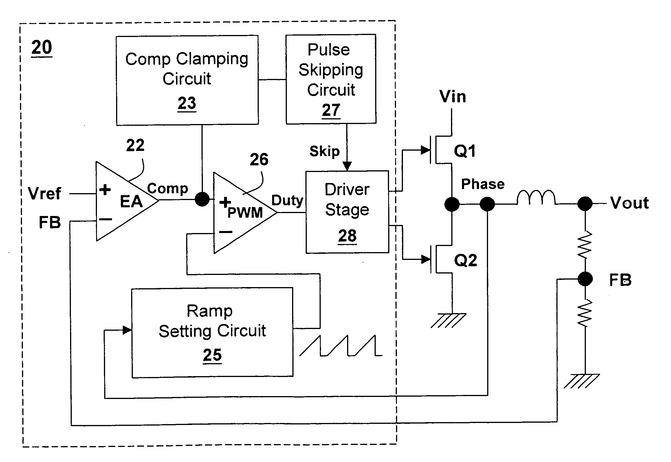
[0039]Referring to FIG. 9, the present invention is illustrated with a buck converter as an example. The switching regulator in this embodiment comprises a control circuit 20, which controls the operation of the power transistors Q1 and Q2 to convert electrical power from the input Vin to the output Vout. The control circuit 20 includes an error amplifier 22, a PWM comparator 26, a driver stage 28, an error amplification signal clamping circuit 23, a Ramp setting circuit 25 and a pulse skipping circuit 27. The error amplification signal clamping circuit (Comp clamping circuit) 23 determines the minimum level Comp_Min according to the level of the signal COMP in CCM or in a stable state. The Ramp setting circuit 25 is for generating a signal Ramp whose slope varies in accordance with the input voltage Vin. The Pulse skipping circuit 27 is for generating a pulse skipping signal Skip to trigger the pulse skipping mode.
[0040]The error amplification signal clamping circuit 23 and the Ram...
second embodiment
[0048]FIG. 15 shows the pulse skipping circuit 27. In the embodiment, a transistor 271 and the transistor 272 constitute a current mirror, which is another way to sense the current through the transistor 236. Similarly, when the current through the transistor 272 is higher than the current of the current source 273, the level of node B is high; when the current through the transistor 272 is lower than the current of the current source 273, the level of node B is low. In this embodiment, the signal at node B first passes through a hysteresis gate circuit 274, and then serves as the pulse skipping signal Skip; in this way, it can reduce noises in the signal and adjust the signal to an appropriate level.
third embodiment
[0049]FIG. 16 shows the pulse skipping circuit 27. In this embodiment, a delay circuit 275 is provided after the hysteresis gate circuit 274. The delay circuit 275 is to prevent the switching regulator from immediately switching to the pulse skipping mode when the signal Comp barely touches the minimum level Comp_Min, to prevent the signal Duty from being too short or unstable. With the delay circuit 275, the switching regulator enters the pulse skipping mode after the signal Comp reaches the minimum level Comp_Min for a period of time, or after at least one switching cycle of the power switches. The delay circuit 275 can be directly connected to the node B if no hysteresis gate circuit 274 is provided in the circuit.
[0050]An example of the delay circuit 275 is shown in FIG. 17, which is constituted by an SR flip-flop. The signal Duty is the clock input of the SR flip-flop, so that the pulse skipping signal Skip outputted from the SR flip-flop is delayed by one switching cycle of th...
PUM
 Abstract
Description
Claims
Application Information
 - R&D
- Intellectual Property
- Life Sciences
- Materials
- Tech Scout
- Unparalleled Data Quality
- Higher Quality Content
- 60% Fewer Hallucinations
Browse by: Latest US Patents, China's latest patents, Technical Efficacy Thesaurus, Application Domain, Technology Topic, Popular Technical Reports.
© 2025 PatSnap. All rights reserved.Legal|Privacy policy|Modern Slavery Act Transparency Statement|Sitemap|About US| Contact US: help@patsnap.com


