Pattern data creating method, computer program product, and semiconductor device manufacturing method

a technology which is applied in the field of creating method and creating method of pattern data, which can solve the problems of becoming difficult to form pattern shapes as per the design on a wafer, becoming increasingly difficult to perform mask manufacturing or wafer processing in order to form micropatterns with precision, and being difficult to form pattern shapes accurately on a wafer

Inactive Publication Date: 2010-07-22
KK TOSHIBA
View PDF12 Cites 1 Cited by
  • Summary
  • Abstract
  • Description
  • Claims
  • Application Information

AI Technical Summary

Problems solved by technology

Moreover, it is becoming difficult to perform mask manufacturing or wafer processing in order to form micropatterns with precision.
For that reason, even if mask patterns having the same shape as the designed patterns are used, it is becoming increasingly difficult to form the pattern shapes as per the design on a wafer.
However, by only adjusting the pattern coverage ratio as described in the abovementioned conventional technology, it was not possible to form patterns of accurate shapes on a wafer.
This problem is attributed to the fact that, due to the difference in the occupancy of cells formed on a wafer, the attached amount of a side wall protective film or the etching time differs thereby resulting in variability in the processing conversion difference.
That causes an increase in the development turnaround time (TAT).

Method used


Image

  • Pattern data creating method, computer program product, and semiconductor device manufacturing method
  • Pattern data creating method, computer program product, and semiconductor device manufacturing method
  • Pattern data creating method, computer program product, and semiconductor device manufacturing method

Examples


Embodiment Construction

[0022]Exemplary embodiments of a pattern data creating method, a computer program product, and a semiconductor device manufacturing method according to the present invention will be explained below in detail with reference to the accompanying drawings. The present invention is not limited to the following embodiments.

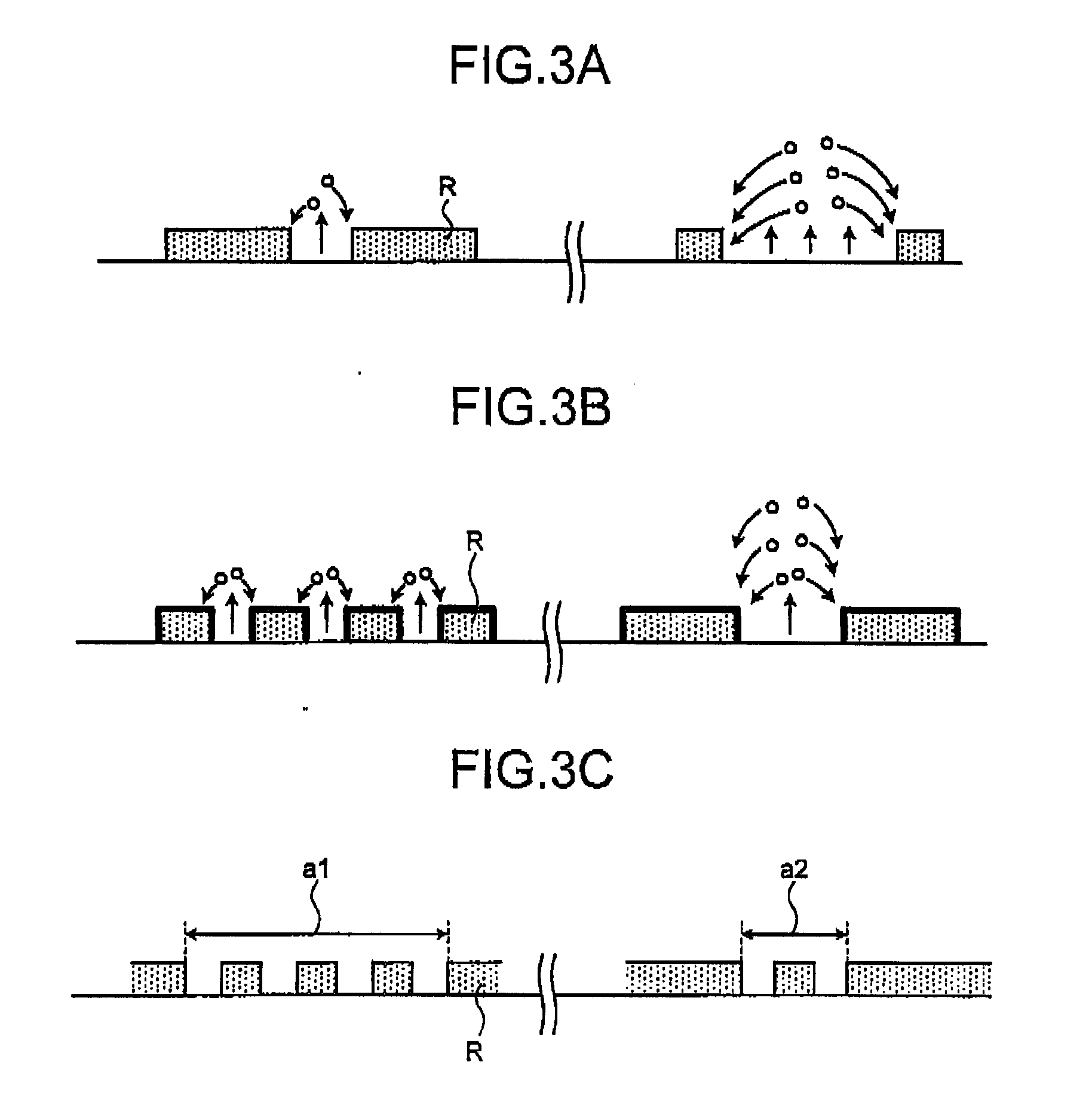
[0023]FIG. 1 is a schematic diagram of a configuration of a pattern data creating apparatus according to the present embodiment. A pattern data creating apparatus 100 is an apparatus such as a computer that creates mask pattern data of a photo mask used in photolithography as a semiconductor device manufacturing process or that creates pattern data of a template used in imprint lithography. In the present embodiment, the description is given about an apparatus for creating mask pattern data of a photo mask used in photolithography and about a method using that apparatus. The pattern data creating apparatus 100 according to the present embodiment calculates an etching co...


PUM

PropertyMeasurementUnit
total surface areaaaaaaaaaaa
shapeaaaaaaaaaa
sizesaaaaaaaaaa

Abstract

A pattern data creating method comprising: referring to a first correspondence relation between an amount of dimension variation between a first pattern formed on a substrate and a second pattern formed by processing the substrate using the first pattern and either one of a pattern total surface area and a pattern boundary length of the first pattern; and creating pattern data for forming the first pattern.

Description

CROSS-REFERENCE TO RELATED APPLICATIONS[0001]This application is based upon and claims the benefit of priority from the prior Japanese Patent Application No. 2009-8135, filed on Jan. 16, 2009; the entire contents of which are incorporated herein by reference.BACKGROUND OF THE INVENTION[0002]1. Field of the Invention[0003]The present invention relates to a pattern data creating method, a computer program product, and a semiconductor device manufacturing method.[0004]2. Description of the Related Art[0005]In recent years, there has been a striking progress in the semiconductor manufacturing technology and semiconductor device of the 50 nm half-pitch generation are being mass-produced. The miniaturization of semiconductor device symbolized by the 50 nm half-pitch generation is achieved by significant advance in the micropattern forming technology such as the mask processing technology, the lithography processing technology, and the etching processing technology. In the times when patte...

Claims


Application Information

Patent Timeline
Patent Type & Authority Applications(United States)
IPC IPC(8): G06F17/50G03F1/68G03F1/70H01L21/027
CPCG03F1/36G03F1/54G03F1/80
Inventor MASHITA, HIROMITSUIYANAGI, KATSUMITAGUCHI, TAKAFUMIKOTANI, TOSHIYAMUKAI, HIDEFUMIUNO, TAIGANAKAZAWA, TAKASHI
Owner KK TOSHIBA
Why Eureka
Try Eureka