Semiconductor memory apparatus and a method for reading data stored therein

a memory apparatus and semiconductor technology, applied in the field of semiconductor memory apparatus, can solve the problems of increasing the number, reducing the performance of the semiconductor memory apparatus, and generating noise and misoperation, so as to reduce the current consumption

Active Publication Date: 2010-06-24
SK HYNIX INC
View PDF4 Cites 13 Cited by
  • Summary
  • Abstract
  • Description
  • Claims
  • Application Information

AI Technical Summary

Benefits of technology

[0009]A semiconductor memory apparatus which may solve the difficulties in interfacing among chips so that data inversion can be performed not only in a DBI mode but also in a no...

Problems solved by technology

However, in the case of semiconductor memory apparatuses operating at a high frequency band, the performance of the semiconductor memory apparatuses may be degraded due to the noise of data.
Nevertheless, the problems caused due to the fact that noise is generated and misoperation occurs due to the increase in the number of data switching times at a high frequency band, have not been solved yet.
However, in the conventional semiconductor memory apparatus 10, because the decision as to whether to invert data is not made unti...

Method used


Image

  • Semiconductor memory apparatus and a method for reading data stored therein
  • Semiconductor memory apparatus and a method for reading data stored therein
  • Semiconductor memory apparatus and a method for reading data stored therein

Examples


Embodiment Construction

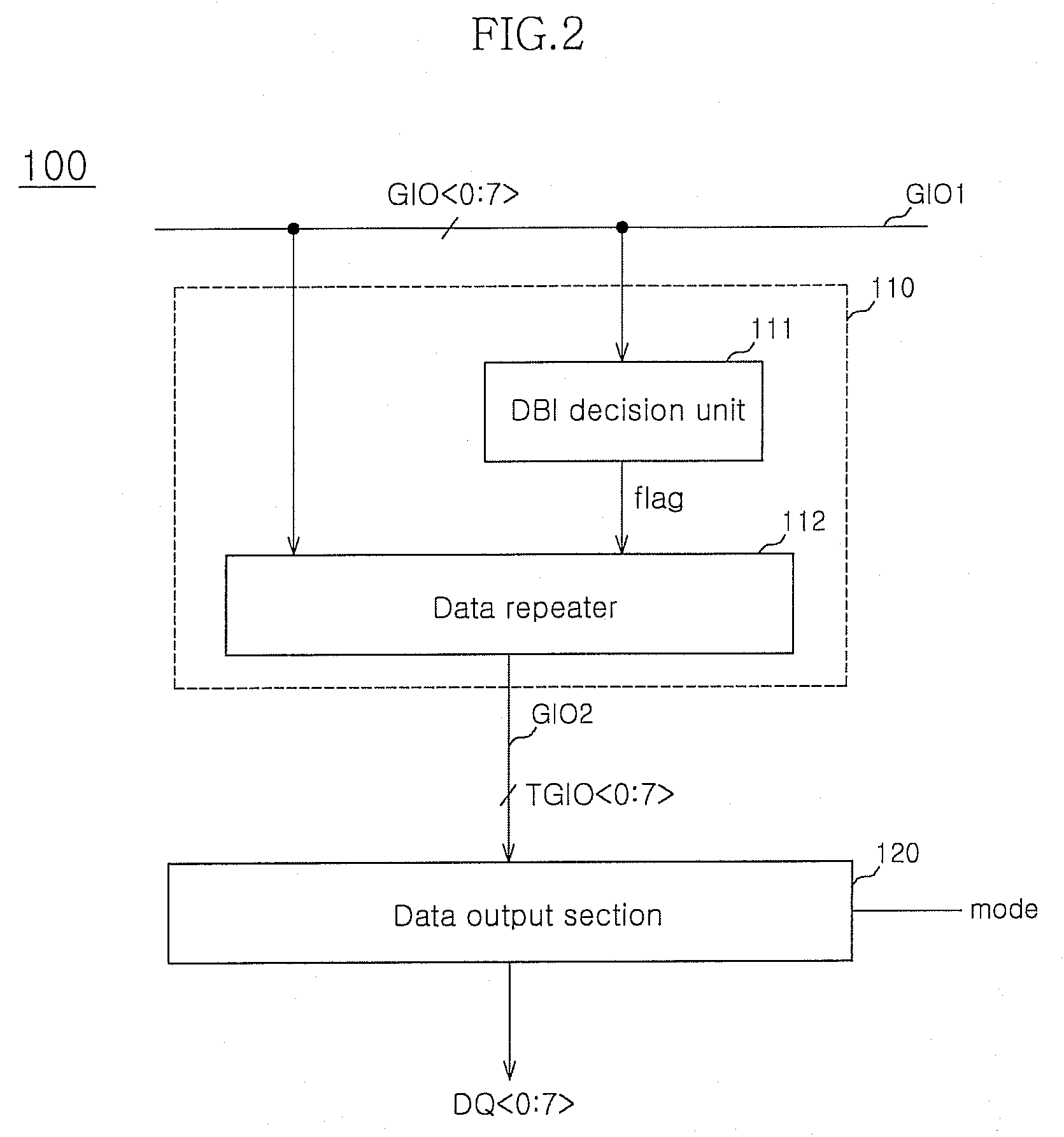
[0019]FIG. 2 is a schematic diagram illustrating the configuration of an exemplary semiconductor memory apparatus in accordance with a first embodiment of the present invention. Referring to FIG. 2, a semiconductor memory apparatus 100 in accordance with a first embodiment can include a data bus inversion (DBI) section 110 and a data output section 120.

[0020]The DBI section 110 can be configured to receive a plurality of data ‘GIO’, decide whether to invert the plurality of data ‘GIO’ depending upon the logic levels of the plurality of data ‘GIO’, to generate a plurality of inversion data ‘TGIO’. In FIG. 2, the DBI section 110 can include a DBI decision unit 111 and a data repeater 112. The DBI decision unit 111 can be configured to receive the plurality of data ‘GIO’ from a data input and output line GIO1 and decide whether to invert or not invert the plurality of data ‘GIO’. The DBI decision unit 111 can generate a decision signal ‘flag’ for deciding whether to invert the pluralit...


PUM


Abstract

A semiconductor memory apparatus includes a data bus inversion (DBI) section configured to receive a plurality of input data and decide whether to invert or output, without an inversion, the plurality of input data depending upon logic levels of the plurality of data, and further configured to generate a plurality of inversion data based on the decision; and a data output section configured to receive the plurality of inversion data, invert or output, without an inversion the plurality of inversion data in response to a mode signal, and generate a plurality of output data.

Description

CROSS-REFERENCES TO RELATED APPLICATION[0001]The present application claims priority under 35 U.S.C. §119(a) to Korean application number 10-2008-0133351, filed on Dec. 24, 2008, in the Korean Intellectual Property Office, which is incorporated herein by reference in its entirety as set forth in full.BACKGROUND[0002]1. Technical Field[0003]The present invention relates to a semiconductor memory apparatus, and, more particularly, to a semiconductor memory apparatus which adopts a data bus inversion scheme and a method for reading data stored in a semiconductor memory apparatus.[0004]2. Related Art[0005]As the data processing speeds of a central processing unit (CPU) and a graphic processing unit (GPU) gradually increase, semiconductor memory apparatuses operating at high frequencies are necessarily demanded in the art. However, in the case of semiconductor memory apparatuses operating at a high frequency band, the performance of the semiconductor memory apparatuses may be degraded du...

Claims


Application Information

Patent Timeline
IPC IPC(8): G11C7/00G11C8/00
CPCG11C7/02G11C7/1048G11C7/1006G11C7/10G11C7/22
Inventor KWAK, SEUNG WOOKKIM, KWAN WEON
Owner SK HYNIX INC
Why Eureka
Try Eureka