Thin film transistor and display device
a thin film transistor and display device technology, applied in the direction of transistors, semiconductor devices, electrical devices, etc., can solve problems such as deteriorating display quality, and achieve the effects of low carrier mobility, large current, and high carrier mobility
- Summary
- Abstract
- Description
- Claims
- Application Information
AI Technical Summary
Benefits of technology
Problems solved by technology
Method used
Image


Examples
embodiment 1
[0045]In this embodiment, a thin film transistor according to an embodiment of the present invention will be described with reference to drawings.
[0046]FIGS. 1A and 1B illustrate a thin film transistor of this embodiment.
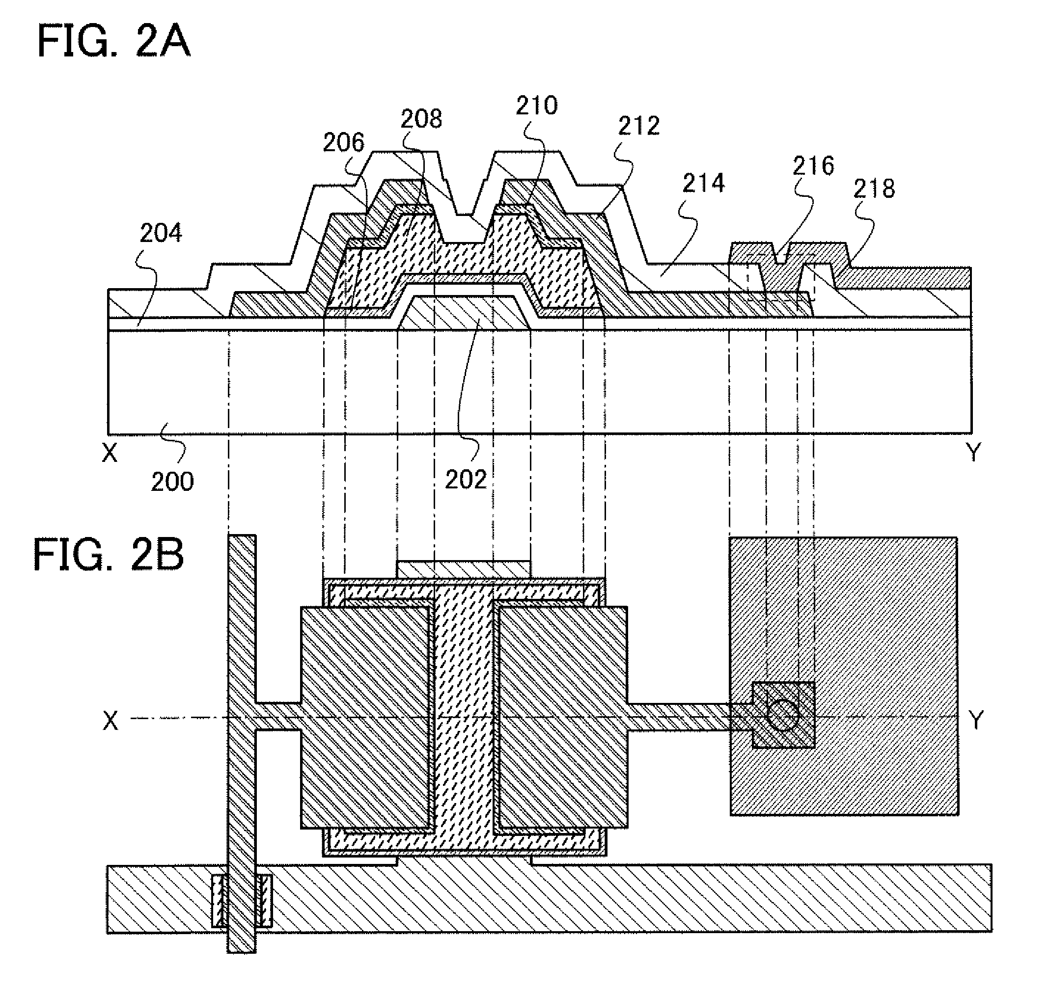
[0047]A thin film transistor illustrated in FIGS. 1A and 1B includes: a gate electrode layer 102; a semiconductor layer (a first semiconductor layer 106 and a second semiconductor layer 108); a gate insulating layer 104 which is provided between and in contact with the gate electrode layer 102 and the semiconductor layer; first impurity semiconductor layers 110 which are provided so as to be in contact with the second semiconductor layer 108; second impurity semiconductor layers 111 each of which is provided so as to be partially in contact with the first impurity semiconductor layer 110 and the semiconductor layer; and source and drain electrode layers 112 which are provided on and in contact with the second impurity semiconductor layers 111. An entire surface of t...
embodiment 2
[0164]In this embodiment, a display device or a light-emitting device which includes the thin film transistor described in Embodiment 1 according to an embodiment of the present invention will be described with reference to the drawings.
[0165]In the display device or the light-emitting device according to this embodiment, a signal line driver circuit and a scan line driver circuit may be formed over a different substrate (for example, a semiconductor substrate or an SOI substrate) and then connected to the pixel portion or may be formed over the same substrate as a pixel circuit.
[0166]Note that there are no particular limitations on the connection method of a substrate separately formed: a known method such as a COG method, a wire bonding method, or a TAB method can be used. Further, a connection position is not limited as long as electrical connection is possible. Moreover, a controller, a CPU, a memory, and / or the like may be formed separately and connected to the pixel circuit.
[0...
embodiment 3
[0191]In this embodiment, an electronic device on which the display device described in Embodiment 2 is mounted will be described with reference to the drawings. Examples of such an electronic device include a television set (also referred to as a television or a television receiver), a monitor of a computer, electronic paper, a camera such as a digital camera or a digital video camera, a digital photo frame, a mobile phone set (also referred to as a mobile phone or a mobile phone device), a portable game machine, a portable information terminal, an audio reproducing device, a large-sized game machine such as a pachinko machine, and the like.
[0192]As an example of the electronic device, electronic paper is given. Electronic paper can be used for electronic devices of a variety of fields as long as they can display data. For example, electronic paper can be used for an electronic book device (e-book), posters, advertisement in vehicles such as trains, display of data on a variety of ...
PUM
 Abstract
Description
Claims
Application Information
 - R&D
- Intellectual Property
- Life Sciences
- Materials
- Tech Scout
- Unparalleled Data Quality
- Higher Quality Content
- 60% Fewer Hallucinations
Browse by: Latest US Patents, China's latest patents, Technical Efficacy Thesaurus, Application Domain, Technology Topic, Popular Technical Reports.
© 2025 PatSnap. All rights reserved.Legal|Privacy policy|Modern Slavery Act Transparency Statement|Sitemap|About US| Contact US: help@patsnap.com