
Anti-tombstoning lead free alloys for surface mount reflow soldering

a lead free alloy and surface mount technology, applied in the direction of soldering apparatus, sustainable manufacturing/processing, final product manufacturing, etc., can solve the problems of easy disturbance of the surface tension of molten solder on the component, rapid increase of tombstoning defects, and toxic effects, etc., to reduce the effect of tombstoning

Inactive Publication Date: 2010-05-13
INDIUM CORP
View PDF0 Cites 12 Cited by
  • Summary
  • Abstract
  • Description
  • Claims
  • Application Information

AI Technical Summary

Problems solved by technology

As the electronics industries continue to pursue miniaturization of the electronic devices, increasing utilization of the small leadless components such as 0402 (this terminology means that the components are 40 mil×20 mil in size) and 0201 has resulted in a rapid increase in tombstoning defects.
The tombstoning effect is attributed to the imbalance of a pulling force caused by surface tension of molten solders at both ends of a component during reflow soldering.
The intricate balance of the surface tension of the molten solder on the component may be easily disturbed by either the change of the solderability of the component or by differences in melting at the moment solder paste at each end of the component begins to reflow.
Lead is known to have toxic effects and poses environmental and public health risks.
For this reason, federal legislation has imposed strict limitations upon the use of lead and lead-containing compositions.
However, the main problem with the present state of the art in reflow soldering based on the lead-free Sn—Ag—Cu alloys is that usable anti-tombstoning solder alloys have not yet been discovered.
Although Katoh et al. in U.S. Pat. No. 6,554,180 B1 teaches using “twin-peak” alloys with 0.2-1 mass % Ag, balanced with Sn as well as a flux to reduce the tombstoning defects, this alloy range deviates too much from the commonly acceptable Sn—Ag—Cu alloy compositions, and therefore is considered an impractical solution.

Method used


Image

  • Anti-tombstoning lead free alloys for surface mount reflow soldering
  • Anti-tombstoning lead free alloys for surface mount reflow soldering
  • Anti-tombstoning lead free alloys for surface mount reflow soldering

Examples


example 1

Making a Solder

[0070]Soldering is an operation in which metallic parts are joined by a molten solder alloy whose melting temperature is generally below 450° C. There are many varieties of solder alloys based on tin and lead, but most recently, due to concerns about environmental and safety issues, Sn—Ag—Cu alloys have been widely used in soldering for electronics assembly. The technique of making solder paste is to mix solder powder with flux. First, the solder alloys are produced by melting ingredient metal ingots and mixing them into solder alloys. Then, the alloys are further atomized to solder powder by either a gas atomization or centrifugal atomization.

example 2

Soldering of Components

[0071]Soldering using a solder paste is called reflow soldering, which is considered the most widely employed soldering method in current electronic industries. There are generally four steps of reflow soldering. First, the solder paste (which is used to remove the metal oxide, thus allowing the solder to react with the pieces being joined; the solder paste is generally composed of metal powder plus flux or a reducing agent) is printed onto pads on a print circuit board. Second, a component is placed on the solder paste deposits. Third, the solder paste is heated above the melting temperature of the constituent solder alloy, and thus produces molten solder between the component and the pads. Finally, as the molten solders is cooled, solder joints are formed.

example 3

Tombstoning Test of Solder Pastes

[0072]A tombstoning test may be performed using an exaggerated severe soldering condition to produce tombstoning. The conditions are shown as follows:

[0073](a) A 0.25 mm thick stencil is used to produce a thick deposit of solder paste. When a small component is soldered to a pad with a thick deposit of solder, the frequency of tombstoning has been found to be greater.

[0074](b) A vapor phase reflow oven is employed. The oven is full of vapor generated by heating a high boiling point fluid such as freon with coils at the bottom of the oven. As the printed circuit board is placed in the vapor, the solder paste is heated by the hot vapor and results in soldering of the components. Following the removal of the reflowed board, the tombstoned components are counted and the percentage of tombstones with respect to the number of components is used for comparison.

[0075](c) A 20 cm×15.2 cm board with Cu pads is employed for testing the tombstoning effect. Four ...


PUM

PropertyMeasurementUnit
mass fractionaaaaaaaaaa

Abstract

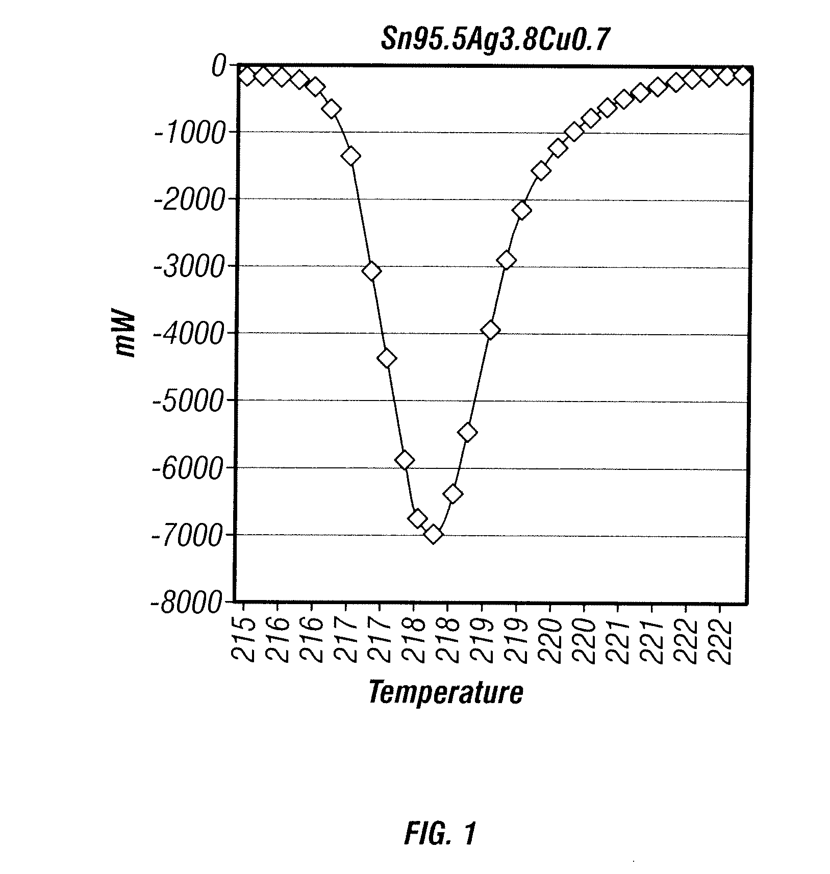
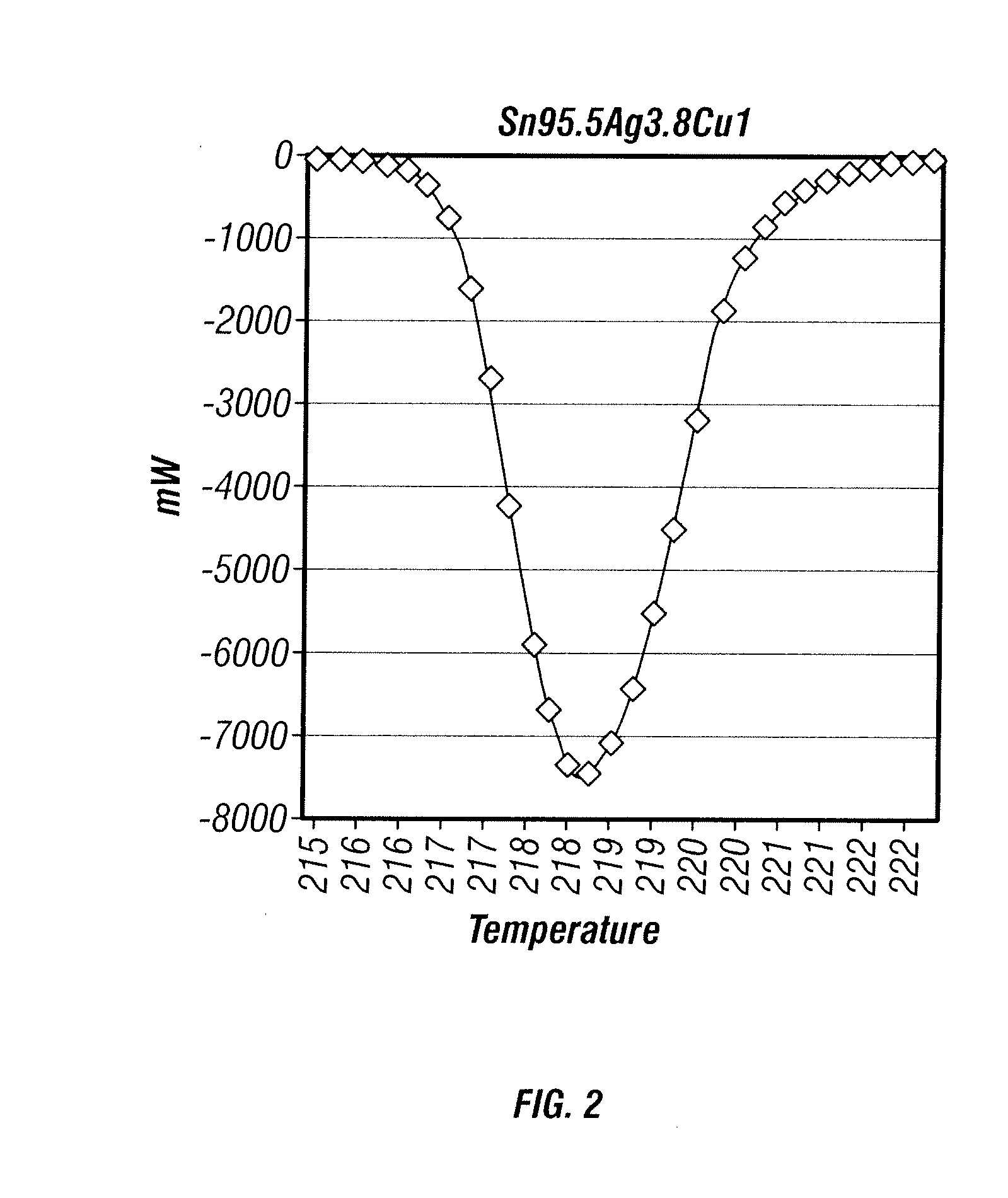
A lead-free solder alloy composition comprising tin, silver and copper, and a process for reflow soldering for minimizing tombstoning frequency are disclosed. In one particular exemplary embodiment, the lead-free Sn—Ag—Cu solder alloys for minimizing the tombstoning effect of the present disclosure display high mass fraction during melting and prolonged melting as shown by a widened DSC peaks, that allows for a balanced surface tension on both ends of the chip component to develop. In accordance with further aspects of this exemplary embodiment, the alloys display a mass fraction of solid during melting greater than 20% and a DSC peak width greater than 8° C. using a 5° C. / min scan rate. In accordance with further aspects of this exemplary embodiment, the alloy comprises on a weight basis Ag 1-4.5%, Cu 0.3-1% balanced with Sn.

Description

CROSS-REFERENCE TO RELATED APPLICATIONS[0001]This patent application claims priority to U.S. Provisional Patent Application No. 60 / 517,404 (Attorney Docket No. 64470.000005); filed Nov. 6, 2003, which is hereby incorporated by reference herein in its entirety.FIELD OF THE DISCLOSURE[0002]The present disclosure relates generally to lead free alloys for use in soldering and, more particularly, to anti-tombstoning alloy compositions comprising tin, silver and copper.BACKGROUND OF THE DISCLOSURE[0003]As the electronics industries continue to pursue miniaturization of the electronic devices, increasing utilization of the small leadless components such as 0402 (this terminology means that the components are 40 mil×20 mil in size) and 0201 has resulted in a rapid increase in tombstoning defects. Such tombstoning defects, which are one of the most common defects observed in surface mount reflow soldering of small leadless components such as resistors and capacitors are caused by a tombstoni...

Claims


Application Information

Patent Timeline
Patent Type & Authority Applications(United States)
IPC IPC(8): B23K35/34B23K1/00B23K35/26C22C13/00H01LH05K3/34
CPCB23K35/262C22C13/00H05K3/3463H05K2201/10636Y02P70/611Y02P70/50
Inventor HUANG, BENLIHLEE, NING-CHENG
Owner INDIUM CORP
Learn More