
Method of forming a metal-insulator-metal capacitor

a metal-insulator and capacitor technology, applied in the direction of capacitors, semiconductor devices, electrical equipment, etc., can solve the problems of anisotropically etching bit line contact holes, increase process complexity and cost, etc., and achieve the effect of increasing the total effective capacitan

Active Publication Date: 2010-05-06
TAIWAN SEMICON MFG CO LTD
View PDF4 Cites 4 Cited by
  • Summary
  • Abstract
  • Description
  • Claims
  • Application Information

AI Technical Summary

Benefits of technology

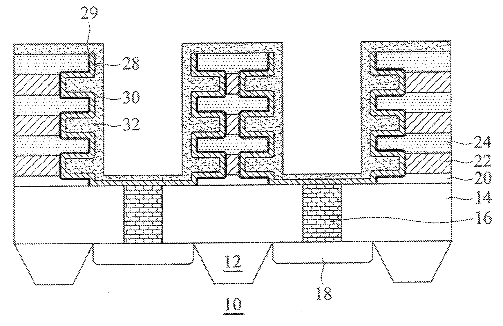
[0005]Embodiments of the present invention include a MIM capacitor structure and a method of forming thereof to increase the total effective capacitance without impacting on bit line contact aspect ratio.

Problems solved by technology

The formation of the thick insulator layer increases process complexity and cost, and causes difficulties in anisotropically etching bit line contact holes with deep and narrow designs.

Method used


Image

  • Method of forming a metal-insulator-metal capacitor
  • Method of forming a metal-insulator-metal capacitor
  • Method of forming a metal-insulator-metal capacitor

Examples


Embodiment Construction

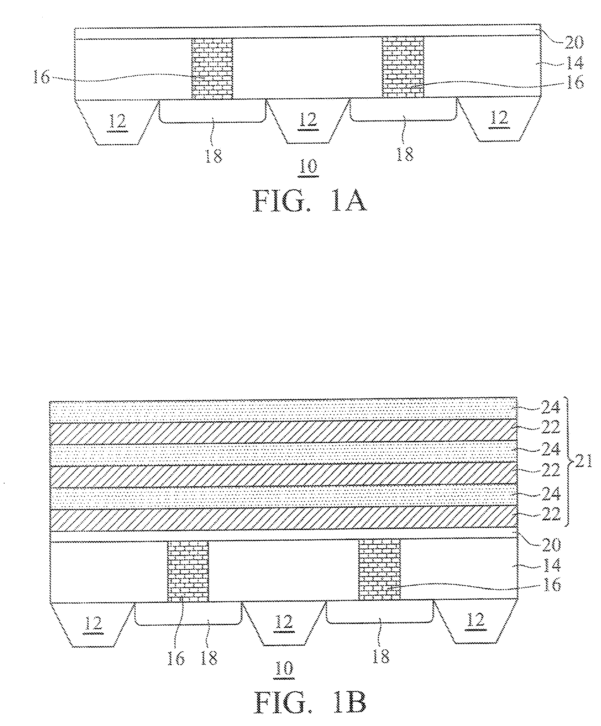
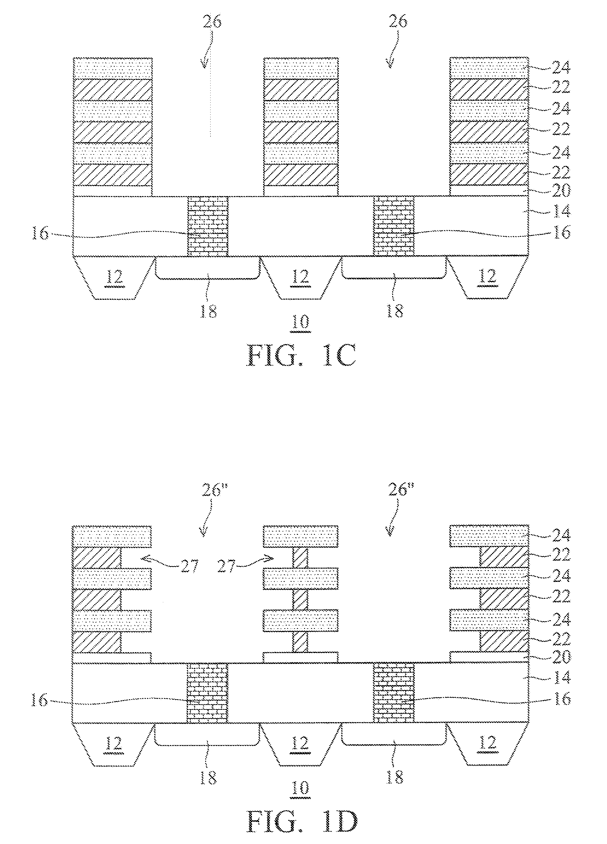
[0011]Embodiments of the present invention provide a MIM capacitor structure and a method of forming thereof. Reference will now be made in detail to the present embodiments, examples of which are illustrated in the accompanying drawings. Wherever possible, the same reference numbers are used in the drawings and the description to refer to the same or like parts. In the drawings, the shape and thickness of one embodiment may be exaggerated for clarity and convenience. This description will be directed in particular to elements forming part of or cooperating more directly with, apparatus in accordance with the present invention. It is to be understood that elements not specifically shown or described may take various forms well known to those skilled in the art. Further, when a layer is referred to as being on another layer or “on” a substrate, it may be directly on the other layer or on the substrate, or intervening layers may also be present.

[0012]Herein, cross-sectional diagrams o...


PUM


Abstract

A method of forming a metal-insulator-metal capacitor has the following steps. A stack dielectric structure is formed by alternately depositing a plurality of second dielectric layers and a plurality of third dielectric layers. A wet etch selectivity of the second dielectric layer relative to said third dielectric layer is of at least 5:1. An opening is formed in the stack dielectric structure, and then a wet etch process is employed to remove relatively-large portions of the second dielectric layers and relatively-small portions of the third dielectric layers to form a plurality of lateral recesses in the second dielectric layers along sidewalls of the opening. A bottom electrode layer is formed to extend along the serrate sidewalls, a capacitor dielectric layer is formed on the bottom electrode layer, and a top electrode layer is formed on the capacitor dielectric layer.

Description

[0001]This application is a Divisional of co-pending application Ser. No. 11 / 640,208, filed on Dec. 18, 2006, the entire contents of which are hereby incorporated by reference and for which priority is claimed under 35 U.S.C. §120.TECHNICAL FIELD[0002]The present invention relates to a method of manufacturing a capacitor of a semiconductor memory, and particularly to a method of forming a metal-insulator-metal (MIM) capacitor structure for a dynamic random access memory (DRAM) device.BACKGROUND[0003]The cell of a semiconductor memory such as a dynamic random access memory (DRAM) device is generally created comprising one single Metal-Oxide-Semiconductor Field-Effect-Transistor (MOS-FET) as a switching device connected with a capacitor as a digital data storage device. A capacitor known as a metal-insulator-metal (MIM) structure possesses a low-interfacial reaction specificity to enhance its performance. The MIM capacitor has therefore become an important topic of research for the me...

Claims


Application Information

Patent Timeline
Patent Type & Authority Applications(United States)
IPC IPC(8): H01L29/92
CPCH01L27/10817H01L27/10852H01L28/86H10B12/318H10B12/033
Inventor TU, KUO-CHI
Owner TAIWAN SEMICON MFG CO LTD
Learn More