Method of manufacturing semiconductor device with embedded interposer
- Summary
- Abstract
- Description
- Claims
- Application Information
AI Technical Summary
Benefits of technology
Problems solved by technology
Method used
Image

Examples
experimental example
[0127]
TABLE 1Solder joint reliability of a semiconductordevice having an embedded interposerSemiconductorEmbeddedSJRCasechip (mm)interposer (mm)CycleImprovementcase 19.1 × 13.84 × 0.55—8221.0case 2 8.8 × 12.8 × 0.19951.2case 3 9.1 × 13.84 × 0.110001.21case 410.16 × 16.76 × 0.110201.24case 5 9.1 × 13.84 × 0.211531.4case 6 9.1 × 13.84 × 0.312761.55
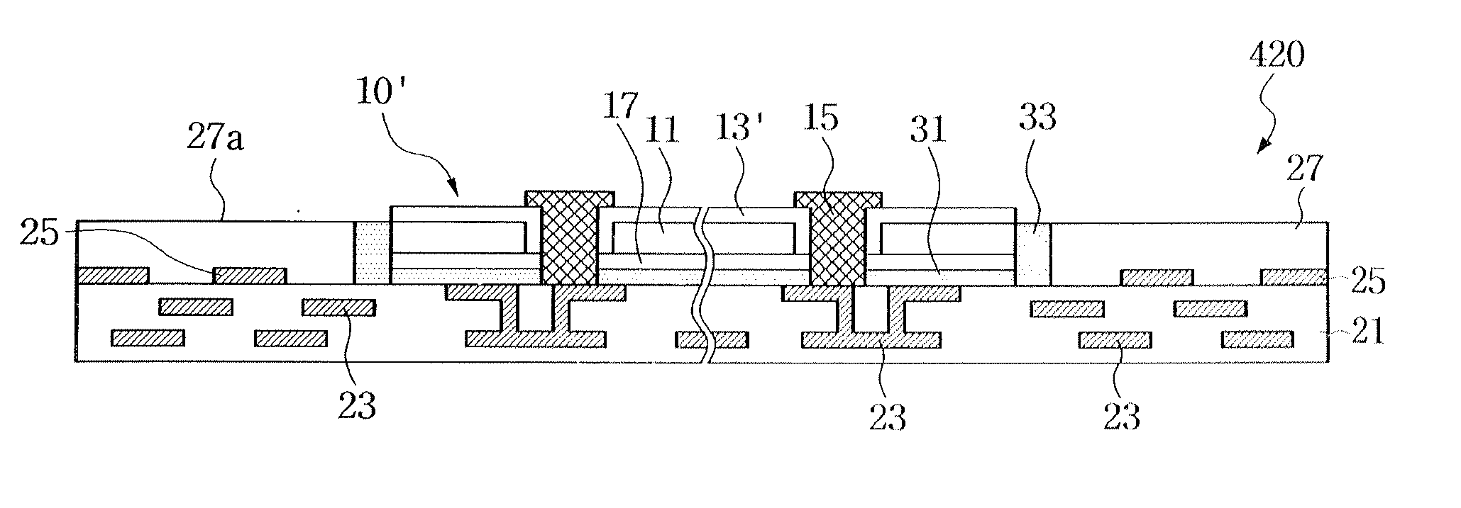
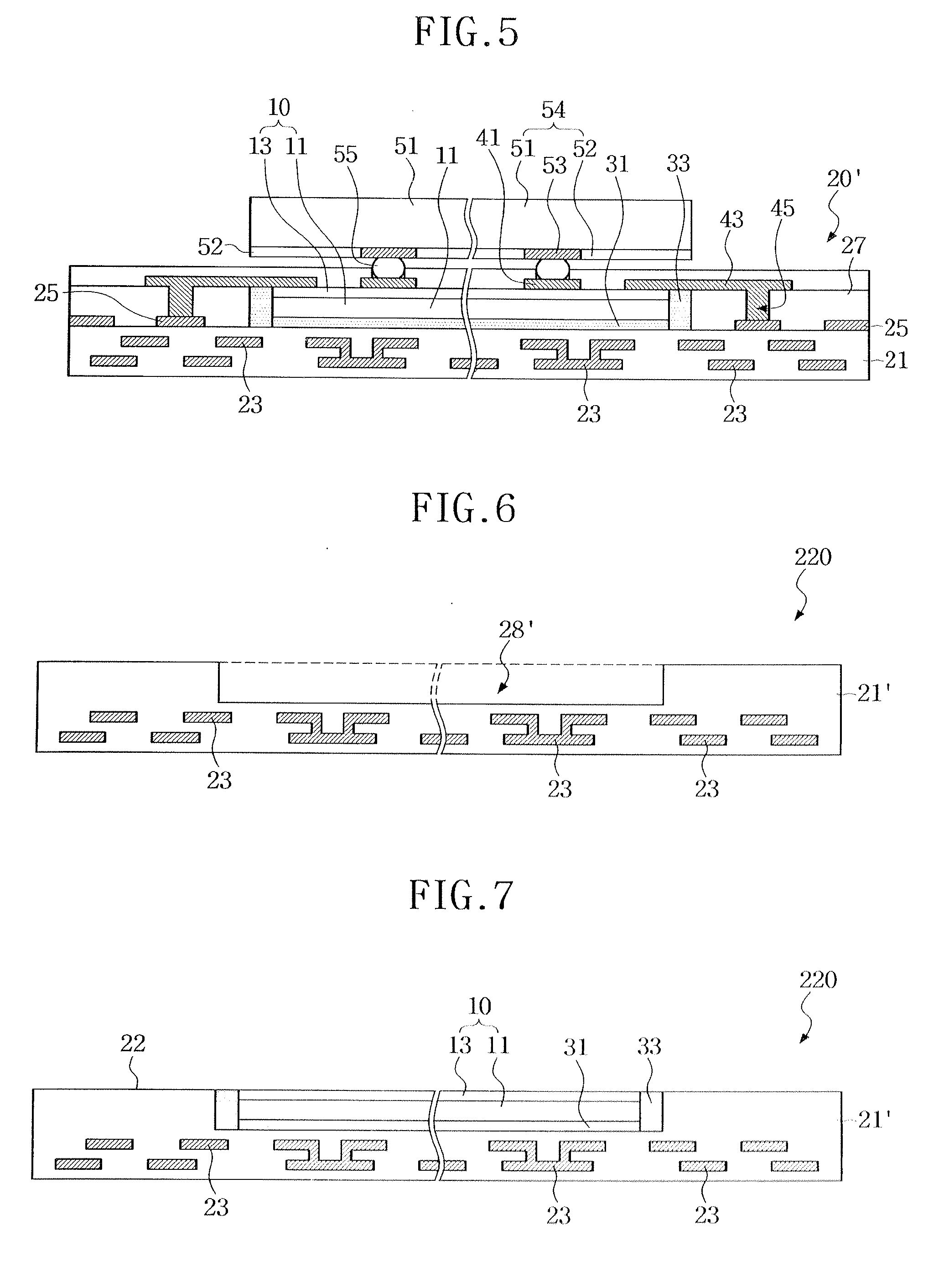
[0128]Table 1 shows solder joint reliability simulation results for a semiconductor device having an embedded interposer according to example embodiments. In the present experimental example, a semiconductor device having a similar configuration to the first example embodiment illustrated in FIG. 5, for example, was used in the simulation. As recorded in Table 1, the WL CSP with semiconductor chips of the same size was used, the embedded interposers had different sizes including different lengths, widths and depts, and a solder ball was used as the conductive adhesive agent. A temperature cycle (T / C) test which is used for a semiconductor re...
PUM
 Abstract
Description
Claims
Application Information
 - R&D
- Intellectual Property
- Life Sciences
- Materials
- Tech Scout
- Unparalleled Data Quality
- Higher Quality Content
- 60% Fewer Hallucinations
Browse by: Latest US Patents, China's latest patents, Technical Efficacy Thesaurus, Application Domain, Technology Topic, Popular Technical Reports.
© 2025 PatSnap. All rights reserved.Legal|Privacy policy|Modern Slavery Act Transparency Statement|Sitemap|About US| Contact US: help@patsnap.com