
NAND Flash Memory Controller Exporting a NAND Interface

a technology of flash memory controller and interface, which is applied in the direction of memory adressing/allocation/relocation, instruments, and semiconductor/solid-state device details, etc., can solve the problems of poor performance, lower reliability of mbc than sbc, and drawbacks to using mbc flash

Active Publication Date: 2010-02-25
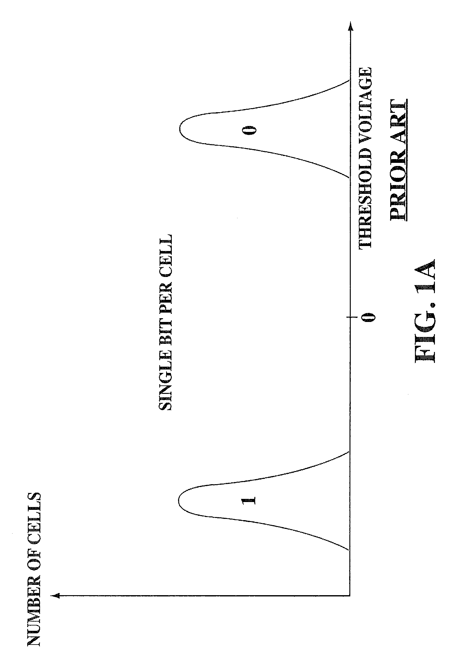
INNOVATIVE MEMORY SYST INC
View PDF94 Cites 10 Cited by
  • Summary
  • Abstract
  • Description
  • Claims
  • Application Information

AI Technical Summary

Problems solved by technology

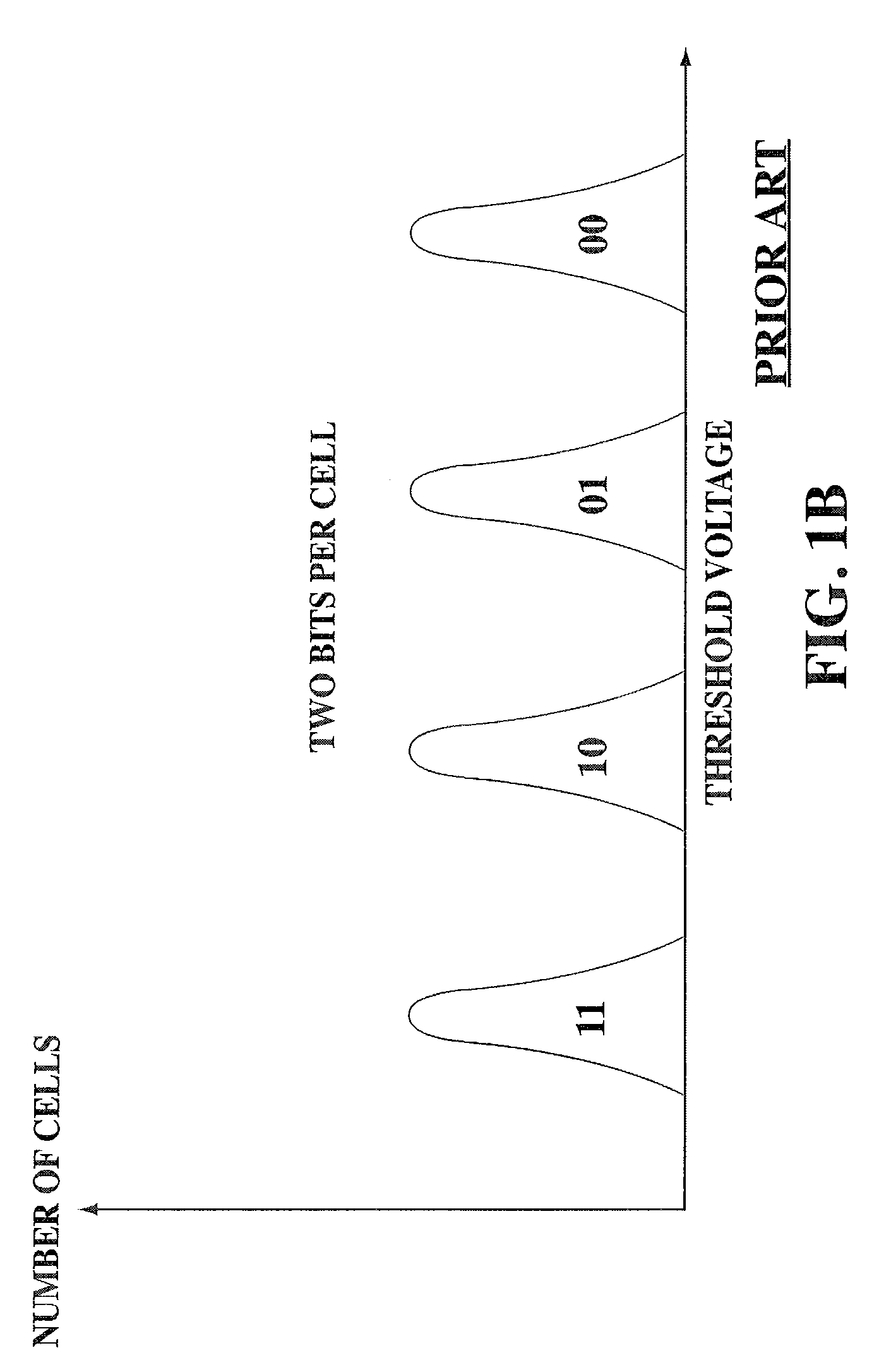
However, there are drawbacks to using MBC flash.
Average read and write times of MBC memories are longer than of SBC memories, resulting in worse performance.
Also, the reliability of MBC is lower than SBC.
Thus, a disturbance in the threshold voltage (e.g. leakage of stored charge causing a threshold voltage drift or interference from operating neighboring cells) that are insignificant in SBC because of the large gap between the two states, may cause an MBC cell to move from one state to another, resulting in an erroneous bit.
The end result is a lower performance specification of MBC cells in terms of data retention time or the endurance of the device to many write / erase cycles.
It is not possible to access any random address in the way described above for NOR—instead the host has to write into the device a sequence of bytes which identifies both the type of the requested command (e.g. read, write, erase, etc.) and the address to be used for that command.
Because of the non-random access of NAND devices, they cannot be used for running code directly from the flash memory.
The SBC and MBC devices are not fully identical in their behavior—the time it takes to write an MBC page is much longer than time it takes to write an SBC page.
Typically, NAND devices are relatively difficult to interface and work with.
Another difficulty is the existence of errors in the data read from NAND devices, In contrast, NOR devices that can be assumed to always return correct data.
This inherent non-reliability of NAND devices requires the use of Error Detection Codes (EDC) and Error Correction Codes (ECC).
However, this architecture suffers from many disadvantages.
First, the host has to individually manipulate each one of the NAND device's control signals (e.g. CLE or ALE), which is cumbersome and time-consuming for the host.
Second, the support of EDC and ECC puts a severe burden on the host parity bits have to be calculated for each page written, and error detection calculations (and sometimes also error correction calculations) must be performed by the host.
All this makes such “no controller” architecture relatively slow and inefficient.
In a system built using this architecture the host processor typically interacts with the NAND controller using some proprietary protocol, as the interaction is internal to the host processor and there is no benefit in using a standard protocol.
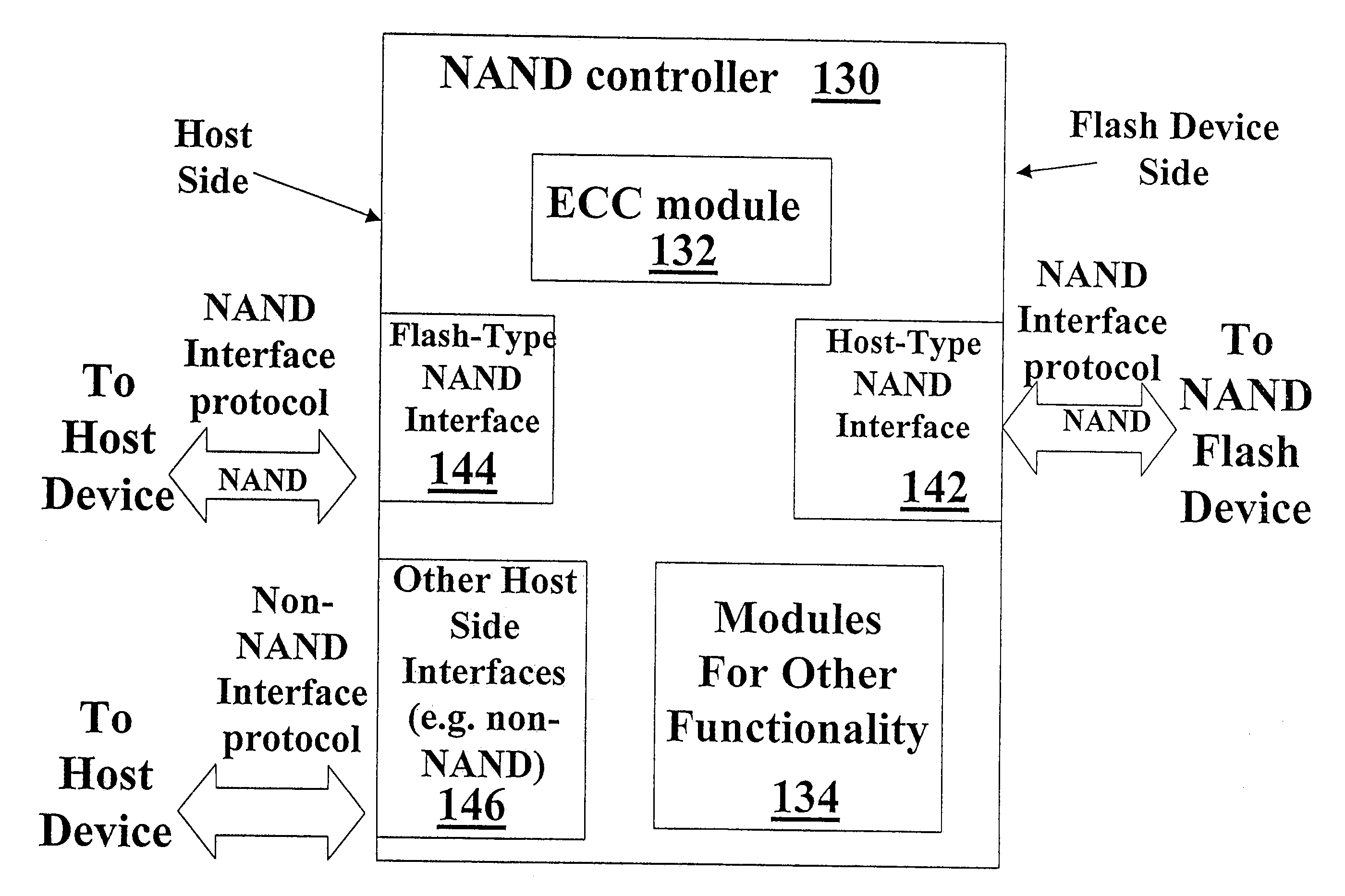
However, one cannot currently find a stand-alone NAND controller that exports NAND interface to the host.
The prior art described above leaves one problem unsolved.
This is so because a NAND controller provides a certain level of error detection and correction, and therefore cannot support NAND devices with lower reliability.
Such controller cannot work with two-bit-per-cell MBC NAND devices because they require 4-bit ECC, and therefore some data might not be read correctly into the processor.
Similarly, a NAND controller providing 4-bit ECC can work with current two-bit-per-cell MBC NAND, but will not work with next generation MBC NAND devices that will most probably require a higher level of ECC capability.
This is so because future MBC NAND devices are expected to be less reliable than current MBC devices and to require a much stronger ECC capability.
With shrinking dimensions of the memory cells comes lower reliability, as the small dimensions make the cells more sensitive to physical effects and phenomena that previously were not important.b. When MBC cells with more than two bits per cell will become commercially available, they will necessarily be much less reliable than SBC cells and two-bit-per-cell MBC cells.
The larger number of states that have to be represented by the cell's threshold voltage imply that the margins between states are smaller and even smaller disturbances and drifts result in incorrect reading of data.
If the MBC NAND is connected to the NAND interface of the built-in controller of the processor, which might be the only way to connect it to the processor, then the MBC NAND generates too many errors for the limited-capability ECC of the built-in controller to correct.
But when NAND devices with lower reliability appear in the market, the processor is not able to benefit from their lower price because its built-in controller is not able to provide the required level of error correction.
Therefore we see that the state of the prior art does not provide a good solution to the problem of benefiting from the cost advantage of a new NAND device, while using a host processor incorporating a built-in NAND controller designed to support a previous generation of NAND devices.

Method used


Image

  • NAND Flash Memory Controller Exporting a NAND Interface
  • NAND Flash Memory Controller Exporting a NAND Interface
  • NAND Flash Memory Controller Exporting a NAND Interface

Examples


Embodiment Construction

[0073]The present invention will now be described in terms of specific, example embodiments. It is to be understood that the invention is not limited to the example embodiments disclosed. It should also be understood that not every feature of the controllers, systems including controllers, and methods of reading and data described is necessary to implement the invention as claimed in any particular one of the appended claims. Various elements and features of devices are described to fully enable the invention. It should also be understood that throughout this disclosure, where a process or method is shown or described, the steps of the method may be performed in any order or simultaneously, unless it is clear from the context that one step depends on another being performed first.

[0074]The present inventor is disclosing for the first time a new type of NAND controller, characterized by the fact that the interface it exports to the host side is a NAND interface. In some embodiments, ...


PUM


Abstract

A NAND controller for interfacing between a host device and a flash memory device (e.g. a NAND flash memory device) fabricated on a flash die is disclosed. In some embodiments, the presently disclosed NAND controller includes electronic circuitry fabricated on a controller die, the controller die being distinct from the flash die, a first interface (e.g. a host-type interface, for example, a NAND interface) for interfacing between the electronic circuitry and the flash memory device, and a second interface (e.g. a flash-type interface) for interfacing between the controller and the host device, wherein the second interface is a NAND interface. According to some embodiments, the first interface is an inter-die interface. According to some embodiments, the first interface is a NAND interface. Systems including the presently disclosed NAND controller are also disclosed. Methods for assembling the aforementioned systems, and for reading and writing data using NAND controllers are also disclosed.

Description

CROSS-REFERENCE TO RELATED APPLICATIONS[0001]This patent application is a divisional of U.S. patent application Ser. No. 11 / 326,336, filed Jan. 6, 2006, which is hereby incorporated by reference and which claims the benefit of U.S. Provisional Patent Application No. 60 / 720,098, filed Sep. 26, 2005.FIELD OF THE INVENTION[0002]The present invention relates to NAND flash memory controllers that export to the host computer the same type of interface that is exported by a standard NAND flash memory device.BACKGROUND OF THE INVENTION[0003]Single Bit and Multi-Bit Flash Memory Cells[0004]Flash memory devices have been known for many years. Typically, each memory cell within a flash memory device stores one bit of information. The traditional way to store a bit in a flash memory cell has been by supporting two states of the memory cell. One state represents a logical “0” and the other state represents a logical “1”.[0005]In a flash memory cell, the two states are implemented by having a flo...

Claims


Application Information

Patent Timeline
Patent Type & Authority Applications(United States)
IPC IPC(8): G06F12/00G06F12/02H05K7/00H01L23/00
CPCG06F11/1068G11C16/04G06F11/1072G06F13/1668G11C16/0483G06F11/1048
Inventor LASSER, MENAHEM
Owner INNOVATIVE MEMORY SYST INC
Learn More