Silicon nitride layer for light emitting device, light emitting device using the same, and method of forming silicon nitride layer for light emitting device
a technology of light emitting devices and silicon nitride layers, which is applied in the direction of semiconductor devices, chemical vapor deposition coatings, coatings, etc., can solve the problems of difficult to directly apply conventional semiconductor processes to the method, involves additional processes and takes a long time, and achieves the effect of simple manners
- Summary
- Abstract
- Description
- Claims
- Application Information
AI Technical Summary
Benefits of technology
Problems solved by technology
Method used
Image
Examples
embodiment 1
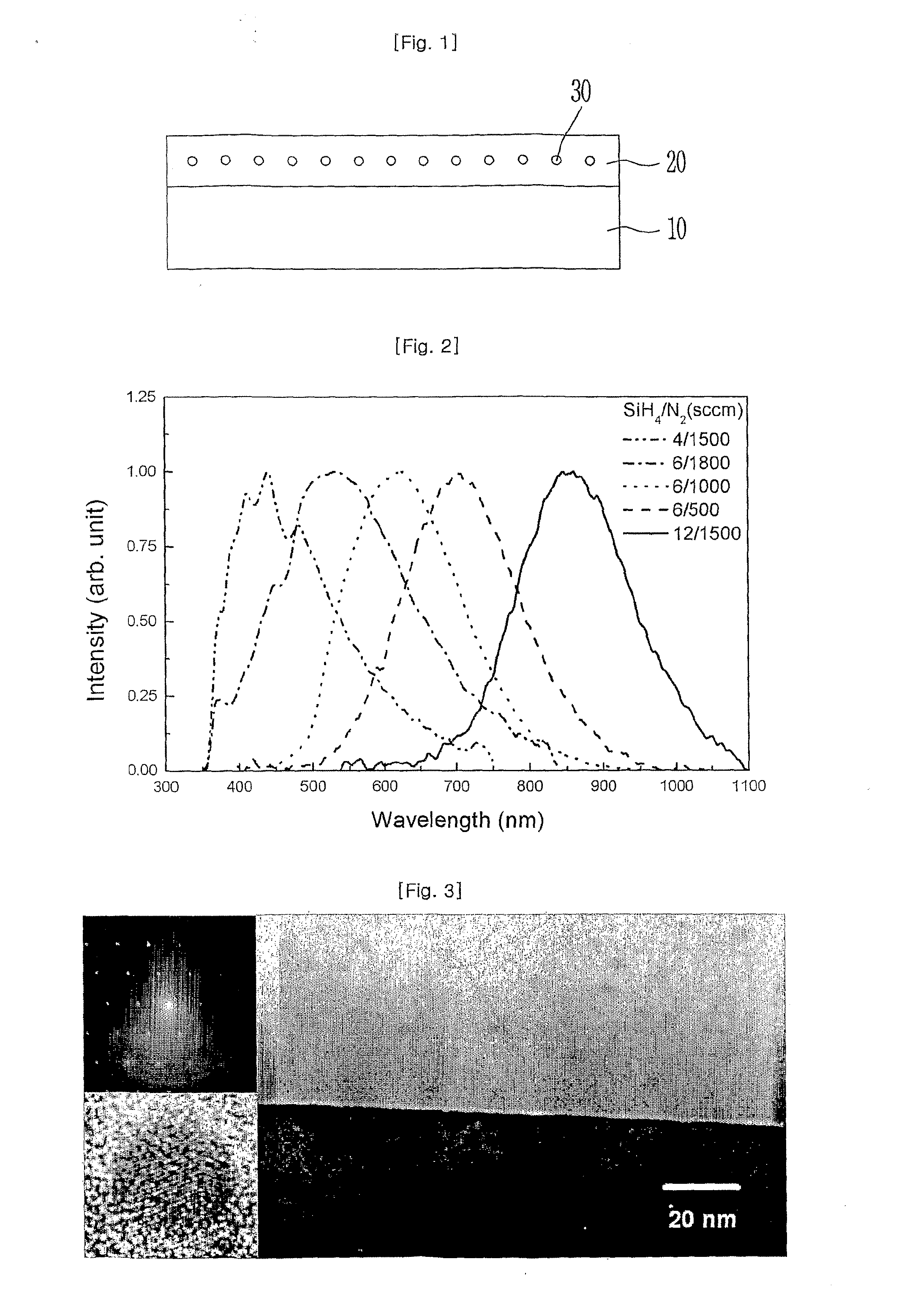
[0029]FIG. 1 is a cross-sectional view illustrating a process of forming a silicon nitride layer for a light emitting device according to an exemplary embodiment of the present invention.
[0030]Referring to FIG. 1, a silicon nitride matrix 20 is formed on a substrate 10, and silicon nanocrystals 30 are formed in the silicon nitride matrix 20.
[0031]The substrate 10 may be, but not limited thereto, a semiconductor substrate such as a silicon (Si) substrate and a germanium (Ge) substrate, a compound semiconductor substrate such as a SiGe substrate, a SiC substrate, a GaAs substrate, and an InGaAs substrate, or an insulating substrate such as a glass substrate, a sapphire substrate, a quartz substrate, and a resin substrate. However, when a silicon nitride layer is formed on a silicon substrate, the silicon substrate has better lattice match. Meanwhile, good lattice match can also be obtained when an additional silicon layer is formed on a substrate other than a silicon substrate and a s...
embodiment 2
[0050]FIG. 6 is a cross sectional view of a silicon light emitting device according to another exemplary embodiment of the present invention.
[0051]Referring to FIG. 6, a silicon emission layer 110 is formed on a predetermined region of a substrate 100, a p-type electrode 120 is formed on another predetermined region of the substrate 100 where the silicon emission layer 110 is not formed. Preferably, the substrate 100 is a ptype silicon substrate.
[0052]The silicon emission layer 110 may be formed using-the above-described silicon nitride layer for the light emitting device according to the first embodiment and includes a silicon nitride matrix and silicon nanocrystals formed in the silicon nitride matrix.
[0053]Meanwhile, an n-type electrode 140 is formed on a predetermined region of the silicon emission layer 110. An n-type doping process may be performed using, for example, a P-based dopant, and a p-type doping process may be performed using, for example, a B-based dopant.
[0054]Also...
PUM
| Property | Measurement | Unit |
|---|---|---|
| pressure | aaaaa | aaaaa |
| temperature | aaaaa | aaaaa |
| diameter | aaaaa | aaaaa |
Abstract
Description
Claims
Application Information
 - R&D
- Intellectual Property
- Life Sciences
- Materials
- Tech Scout
- Unparalleled Data Quality
- Higher Quality Content
- 60% Fewer Hallucinations
Browse by: Latest US Patents, China's latest patents, Technical Efficacy Thesaurus, Application Domain, Technology Topic, Popular Technical Reports.
© 2025 PatSnap. All rights reserved.Legal|Privacy policy|Modern Slavery Act Transparency Statement|Sitemap|About US| Contact US: help@patsnap.com


