Method and apparatus for electroplating

Inactive Publication Date: 2010-02-25
NOVELLUS SYSTEMS
View PDF99 Cites 103 Cited by
  • Summary
  • Abstract
  • Description
  • Claims
  • Application Information

AI Technical Summary

Benefits of technology

[0009]These needs are addressed, in one aspect, by providing an electroplating apparatus and a method for uniform electroplating that make use of an ionically resistive element having electrolyte-permeable pores or holes, where the element resides in close proximity of the wafer substrate. The ionically resistive ionically permeable element described herein substantially improves plating uniformity on thin resistive seed layers. It is particularly useful when employed in combination with an auxiliary cathode configured to divert or remove a portion of current from the anode that would otherwise pass to the edge region of the wafer. In certain embodiments, the auxiliary cathode resides between the ionically resistive ionically permeable element and an anode in the electroplating apparatus. In certain embodiments, the auxiliary cathode is located in this position as a virtual cathode. The ionically resistive ionically permeable element described herein presents a uniform current density in the proximity of the wafer cathode and therefore serves as a virtual anode. Accordingly, the ionically resistive ionically permeable element will be also referred to as a high-resistance virtual anode (HRVA)

Problems solved by technology

These thin films, some having inherently large specific resistivities, present the engineer with an extreme terminal effect situation.
Without appropriate means of resistance and voltage compensation, this large edge-to-center voltage drop could lead to an extremely non-uniform plating thickness distribution, primarily characterized by thicker plating at the wafer edge.
These approaches have significant limitations related to the physical properties of the materials and the processes.
Also, because the conductivity of a plating bath is tied to its ionic concentration and pH, decreasing the conductivity directly and negatively impacts the rate of plating and morphology of the plated material.
The plating electrolyte contained within the pores of the HRVA allows ionic current to pass though the disk, but at a significant voltage drop compared to the system as a whole.

Method used


Image

  • Method and apparatus for electroplating
  • Method and apparatus for electroplating
  • Method and apparatus for electroplating

Examples


Embodiment Construction

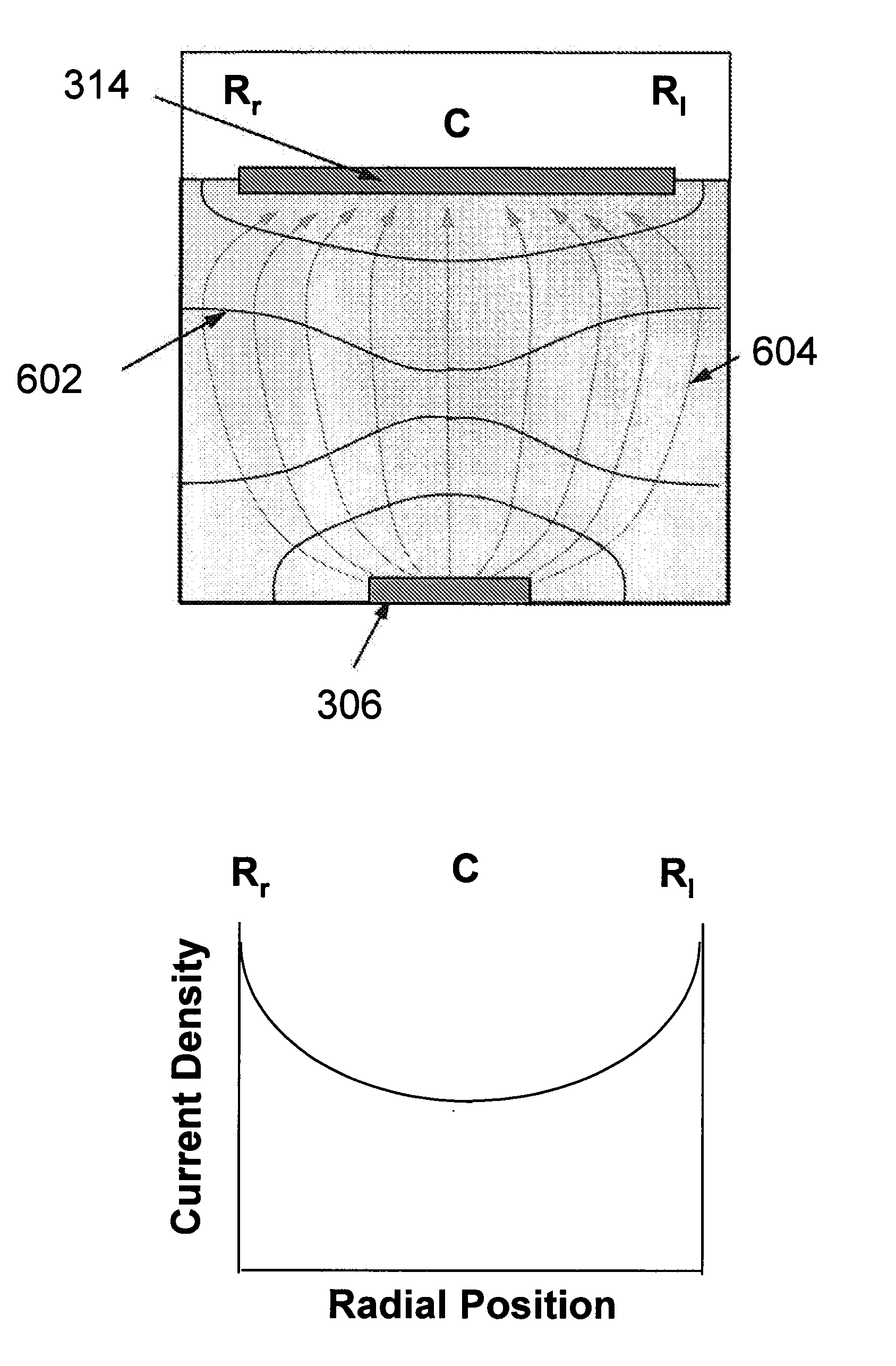
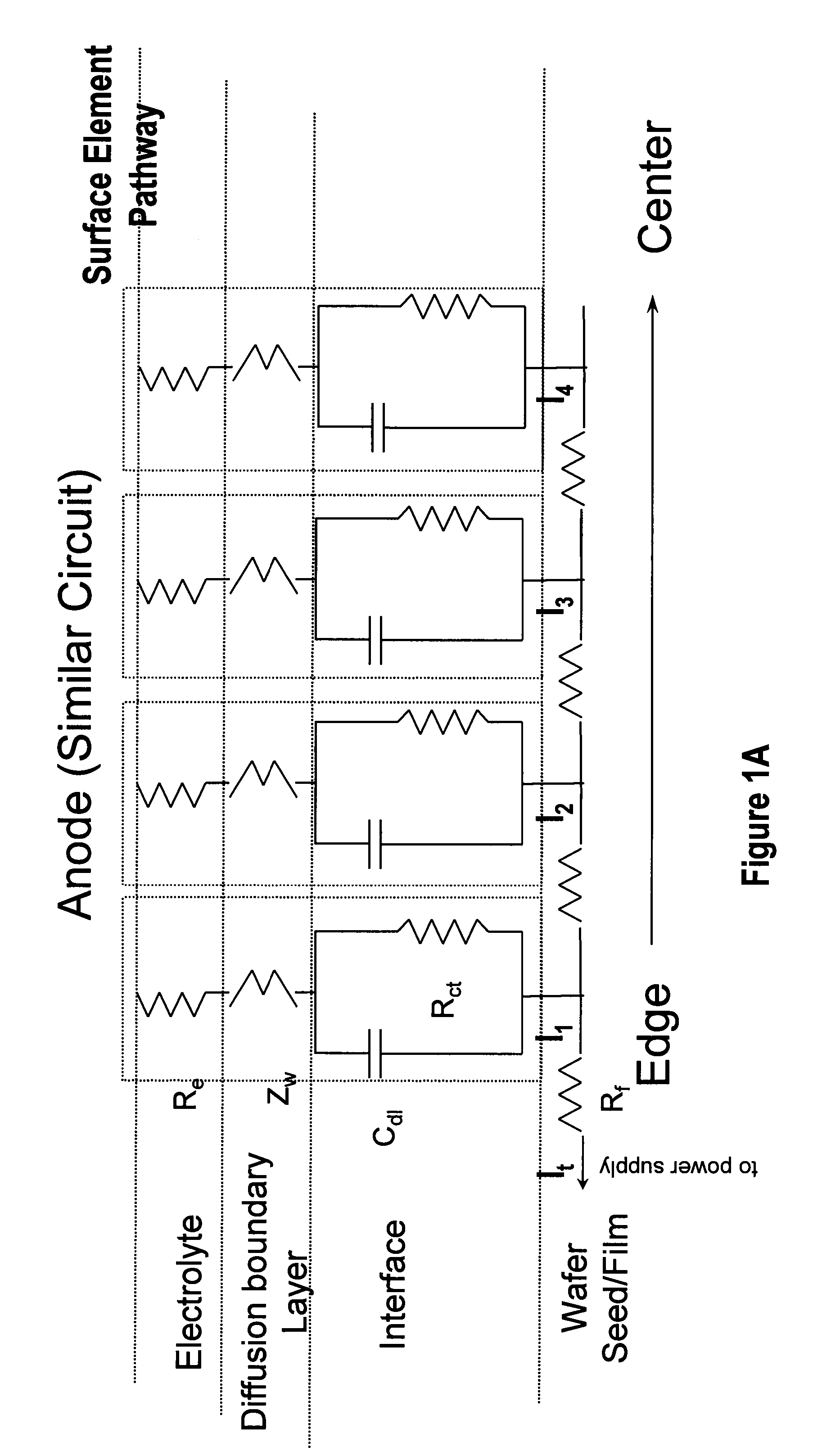
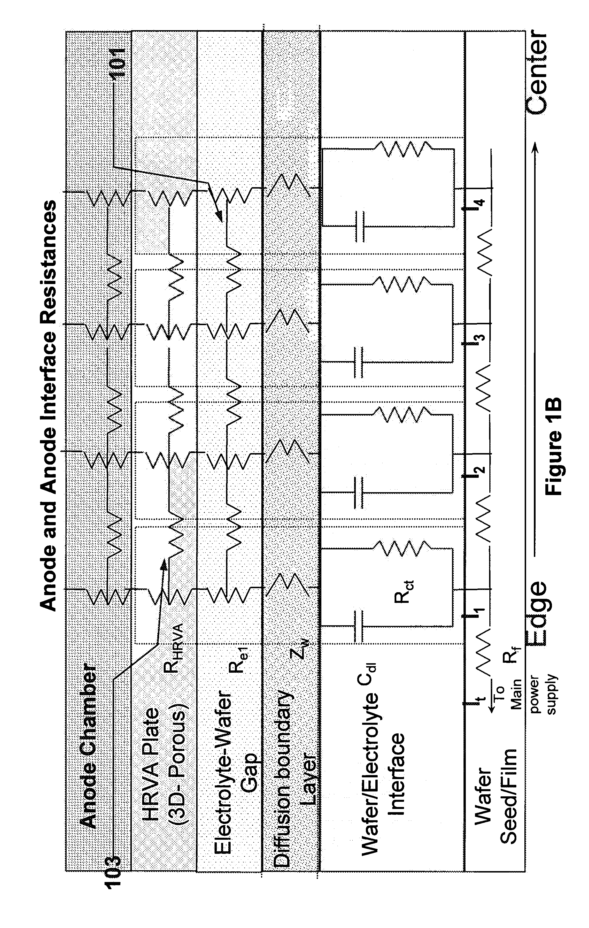
[0029]Advanced technologies call for the electroplating of metals onto wafers with sheet resistances of 10 ohm per square and higher (even 20 ohms per square or 40 ohms per square or higher). This requires ever more aggressive techniques (i.e., techniques other than only the use of a HRVA alone or a thief electrode alone) to compensate for the terminal effect. During plating, the thickness of metal and the sheet resistance can drop several orders of magnitude in a short time, and so methods and apparatus capable of plating uniformly on the wafer throughout a process where there may be a rapidly initially varying and later a relatively constant sheet resistance are required. Embodiments of the present invention address the challenges presented by such high resistance seed layers, the rapid dynamic variance in the seed electrical parameters, and the extreme terminal effect they present.

[0030]Embodiments of the present invention pertain to methods and apparatuses for electroplating a s...


PUM

PropertyMeasurementUnit
Lengthaaaaaaaaaa
Timeaaaaaaaaaa
Diameteraaaaaaaaaa

Abstract

An apparatus for electroplating a layer of metal onto the surface of a wafer includes an ionically resistive ionically permeable element located in close proximity of the wafer and an auxiliary cathode located between the anode and the ionically resistive ionically permeable element. The ionically resistive ionically permeable element serves to modulate ionic current at the wafer surface. The auxiliary cathode is configured to shape the current distribution from the anode. The provided configuration effectively redistributes ionic current in the plating system allowing plating of uniform metal layers and mitigating the terminal effect.

Description

CROSS-REFERENCE TO RELATED APPLICATIONS[0001]This application is a continuation of U.S. patent application Ser. No. 12 / 481,503, filed Jun. 9, 2009, and naming Steven Mayer et al. as inventors, which is in turn a continuation-in part of U.S. patent application Ser. No. 12 / 291,356, filed Nov. 7, 2008, naming Jonathan Reid et al. as inventors, both of which are herein incorporated by reference in its entirety and for all purposes. This application is also a continuation-in-part application of co-pending U.S. patent application Ser. No. 11 / 213,190, filed Aug. 27, 2005, naming S. Mayer et al. as inventors, which is a continuation-in-part application of U.S. patent application Ser. No. 10 / 274,755, filed Oct. 21, 2002, by Contolini et al., titled “Dynamically Variable Field Shaping Element”, now issued as U.S. Pat. No. 7,070,686, which in turn is a continuation-in-part application of U.S. patent application Ser. No. 09 / 542,890 filed Apr. 4, 2000, by Contolini et al., now issued U.S. Pat. N...

Claims


Application Information

Patent Timeline
IPC IPC(8): C25D5/00C25D17/00C25D21/12
CPCC23C18/1601C25D21/14C25D17/002C25D17/007C25D17/008C25F3/30H01L21/2885H01L21/32115H01L21/32125H01L21/6715H01L21/76873C25D17/12C25D21/12C25D17/001C25D5/02C25D17/02C25D17/08C25D17/10H01L21/28
Inventor MAYER, STEVENFENG, JINGBINHE, ZHIANREID, JONATHANVARADARAJAN, SESHASAYEE
Owner NOVELLUS SYSTEMS
Why Eureka
Try Eureka